
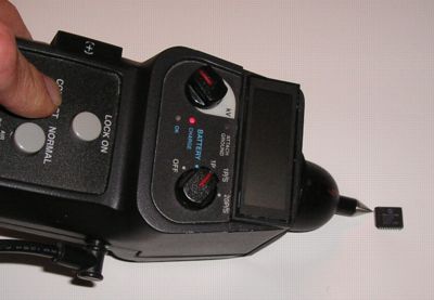
Figure 1. Misapplication of an IEC 61000-4-2 ESD Simulator to a Chip
Abstract: A trend in component testing has been developingin recent years. Vendors of system components are being required by theircustomers, equipment manufacturers, to apply inappropriate system level teststo system components such as chips or modules. One such case of misapplicationof a system test to IC chips is explored and implications discussed.
Discussion: Vendors of system components, such as integrated circuits,are being asked by equipment manufacturers to apply system level tests tosystem components where the test does not apply and often yields uselessresults. Misapplying test standards can lead to extra cost being built intoa product with little or no benefit to the customer. In addition, misunderstandings between vendors and manufacturers can arise because a system level standardlikely gives no guidance as to how the test should be conducted for IC chipsor modules. In the absense of a well thought out written test procedure,the person running the test must essentially invent, on the spot, a testprocedure that would normally be part of the standard governing the testand take years to develop. Unless the test procedure is carefully documentedand made public, the results of the test are of little value as the resultsare strongly affected by the test method used.
In addition to the test procedure specification, one must logically ask ifthe test makes sense for a particular case. For instance, an IC whose connectionsappear on a system connector may already be covered by IEC 61000-4-2 forESD immunity depending on the design of the connector. The test may makeno sense for an IC buried deep within a system with no external connections.Even if an IC has such connections, if there are other components (an ethernettransformer, for instance) between the IC and the external world, IEC 61000-4-2may not apply for that IC.
Let's explore further the misapplication of a system level ESD testto IC chips. IEC 61000-4-2 is an international standard intended to model the discharge from a person holdinga metallic object in a hand to an electronic system. The defined waveshapeof the discharge current into a 1 meter square metal plane is shown in Figure1. The risetime to the first peak (700ps-1ns), the values at the first peakand at 30 and 60 ns are specified. Although intended as an averageof a hand-metal discharge to an electronic system, the actual current will vary considerably in practice.
If IEC 61000-4-2 were applied to an IC chip, the current waveform deliveredto an IC would be strongly dependent on how the IC was connected. If floatingas shown in Figure 1, only a remnant of the initial peak would be observedsince the IC has only a small free space capacitance to charge and noDC/low frequency connections. If one or more of the pins were connected to "ground," muchmore current would flow, but the current would be dependent on the inductance and capacitanceof the connections (which need to be specified).
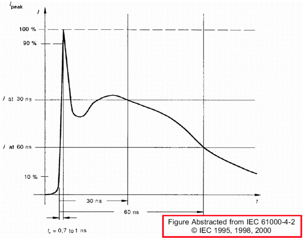
Figure 2. Waveform Specification of an IEC 61000-4-2 ESD Simulator
In addition to current waveform differences, system design will oftendominate differences in IC design with respect to ESD performance of thechip in the system. For instance, an IC chip in the middle of a board with noconnections off the board would be likely be somewhat protected.Whereas, if some of an IC's pins connect to a board edge connector, any dischargeto those pins would result in significantly more current as the board would be chargedthrough the IC. The stress on thechip would be more severe than a chip internal to the board. Other layout issueson the board, such as allowing signal traces to cross ground plane breakscan also significantly increase the stress on an IC from an applied ESDpulse.
Figure 2 shows a test example for a piece of tabletop equipment (somedetails have been removed, see the original standard for the exact test setup)in IEC 61000-4-2. The standard carefully describes how the discharges areto be applied to the external enclosure of the equipment as well as the metaltabletop and the vertical coupling plane, VCP (a metal plane held close tothe system which radiates EMI into the system when the plane is subjectedto a discharge). Criteria for system operation that passes or fails thetest is given. Both equipment damage and soft errors are addressed. But, nothing in the test procedure even hints as to how the discharge would be applied to internal system components.
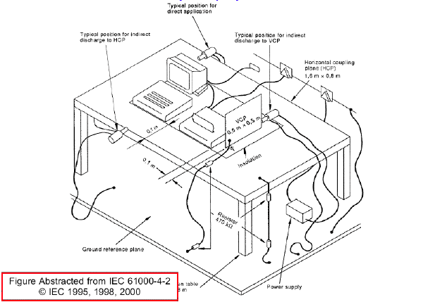
Figure 3. Tabletop Equipment Test Setup for IEC 61000-4-2
Figure 4 shows an air discharge tip (upper) and a contact discharge tip (designedfor discharge to metal surfaces) with some details removed. These tips areon the order of 50 mm long. The standard requires the use of these tips,but how could these be used for IC chip testing? Can you imagine testinga 1200 pin ball grid array package with one of these tips?
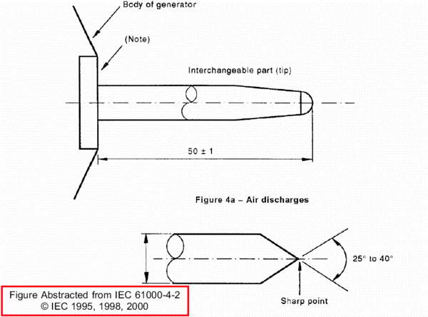
Figure 4. ESD Simulator Tips Used in IEC 61000-4-2
Summary:In general, if a system level ESD test (such as IEC 61000-4-2) is appliedto individual IC chips, test results will be determined by the (often unspecified) procedure used to test the IC chip. In addition, system and board designwill likely be much more important to IC chip survival in the field thanwhether the IC chip survives a misapplied system test. There may be a few cases where IEC 61000-4-2 can be adapted to limited cases of IC testing,but such cases would be rare, include connections between the chip and outsideworld, and require the IEC test be supplemented with a completely new testprocedure.
Applyingan ESD system level test to IC chips and modules adds cost and usually verylittle value to a product. The results of such a test are generally not usefulunless an appropriate test method is specified to adapt the standard to thenew application and a solid technical justification for doing the test exists.
Additional information on this site regarding ESD effects on systems include:
- November 1999: Transient Suppression Plane
- May 2001, Hidden Threatsto Electronic Equipment
- January 2002, Cable Effects Part 1: CableDischarge Events
- May 2002, Printed Wiring Board Coupling toa Nearby Metal Plane, Part 2: ESD Immunity
- February 2003, Crossing Ground Plane Breaks - Part 3, Immunity to Radiated EMI
- May 2003, Signal Paths Passing Through Ground and Power Planes, Effects on Immunity
- ESD Immunity in System Designs, System FieldExperiences and Effects of PWB Layout (~950K)
- (2000 EOS/ESD Symposium paper)