
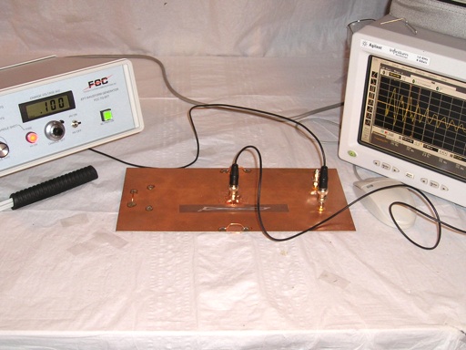
Figure 1. Test Setup For Measuring Voltage Between the Planes on a Four Layer PCB Model
(Measurement in the time domain)
Abstract: Four layer PCBs are
used in a wide variety of applications. However, usually it is
necessary for some signal paths to be routed on both the top and bottom
signal layers to achieve required routing density. Using a model of a
four layer PCB with ground and power planes, data is presented in the time domain that
shows routing signals on both signal layers can cause significant
signal voltage to be developed between the planes unless a simple
design rule is observed.
Discussion: Figure 1 shows the
test setup used to generate data, composed of a Fischer Custom Communications TG-EFT high voltage pulse generator, an Agilent Infinium 54845a scope, and a test board. The test board is copper clad on
both sides and about 50 mils thick. A close-up of the bottom of the
board is shown in Figure 2, before the BNC connector was added in the
middle
of the board. Two paths about 9 inches (~23 cm) in length run from SMA
connectors
to 51 Ohm load resistors. The paths are made from the individual
insulated wires of 100 Ohm twisted pair telephone wire taped down to
the underlying plane, thus forming approximately 50 Ohm transmission
lines. One
path stays on the bottom of the board while the other path runs about
1/3 of its length on the top side of the board (visible in Figure 1).
The two planes are shorted together by the SMA connectors and at the load resistors. This simulates four bypass capacitors between the power and ground planes of a four layer PCB. Most four layer PCBs have more than four bypass capacitors, but I wanted to show a limiting case with only four. The results are worst case compared to most four layer PCBs. However, I have seen PCBs that needed additional bypass capacitors. In addition, passive four layer PCBs with no active components, such as a backplane, sometimes have few if any bypass capacitors.
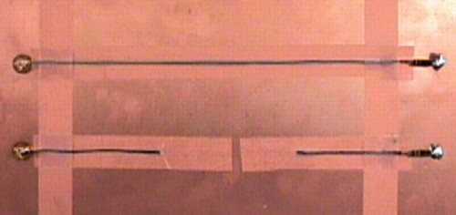
Figure 3 shows a close-up of the top side of the test board. A BNC board mount connector has been soldered down to the top plane (and surrounded by copper tape to insure a good 360 degree contact from the plane to the connector). The center pin of the connector is soldered to the bottom plane so the signal at the BNC connector is the signal voltage between the planes. This connector is connected to the scope input while the TG-EFT pulse generator output is connected to one or the other of the SMA connectors that the signal paths on the bottom of the board are connected to (right side of Figure 3). SMA to BNC adapters are used to interface the BNC cable to the scope.
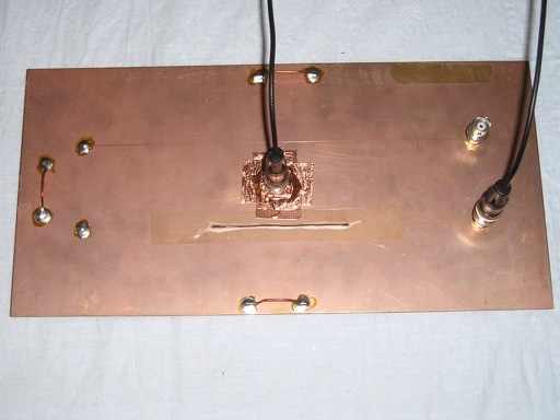
Figure 3. Top Side of Test Board
The two planes are shorted together by the SMA connectors and at the load resistors. This simulates four bypass capacitors between the power and ground planes of a four layer PCB. Most four layer PCBs have more than four bypass capacitors, but I wanted to show a limiting case with only four. The results are worst case compared to most four layer PCBs. However, I have seen PCBs that needed additional bypass capacitors. In addition, passive four layer PCBs with no active components, such as a backplane, sometimes have few if any bypass capacitors.
Figure 2. Bottom Side of Test Board
Figure 3 shows a close-up of the top side of the test board. A BNC board mount connector has been soldered down to the top plane (and surrounded by copper tape to insure a good 360 degree contact from the plane to the connector). The center pin of the connector is soldered to the bottom plane so the signal at the BNC connector is the signal voltage between the planes. This connector is connected to the scope input while the TG-EFT pulse generator output is connected to one or the other of the SMA connectors that the signal paths on the bottom of the board are connected to (right side of Figure 3). SMA to BNC adapters are used to interface the BNC cable to the scope.
Figure 3. Top Side of Test Board
The
TG-EFT was set to produce 100 Volt pulses (with a rise time of 2 ns and
a fall time of about 100 ns). This setting would produce a current
pulse into the signal path on the board of about one Ampere since a 50 Ohm series termination was used on the output of the TG-EFT, similar to that shown in Figure 4, and the rest of the signal path is also 50 Ohms.
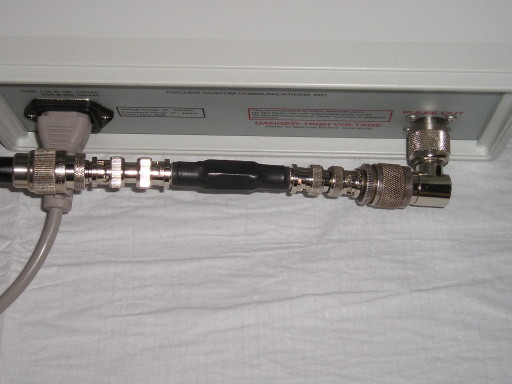
Figure 4. 50 Ohm Series Termination Used With TG-EFT Pulse Generator
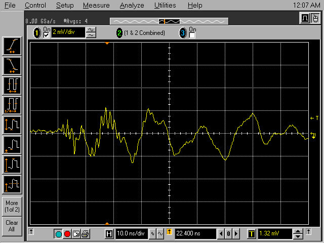
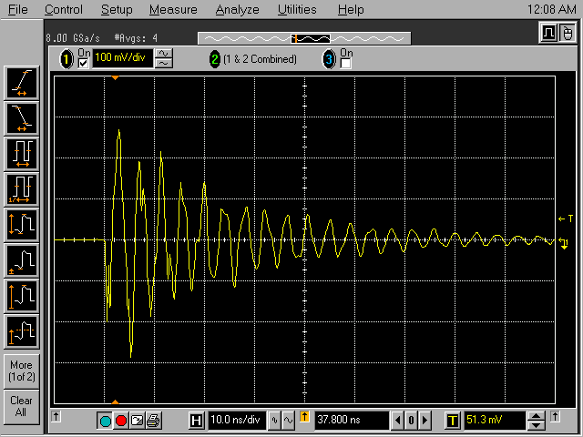
Figures 5 and 6 show the scope plots that resulted when the TG-EFT generator was connected to the path that stayed on one side of the board and the path that was routed on both sides respectively. For the path that stayed on the same side of the board, the plot in Figure 5 shows a peak amplitude of about 2 mV, a very small value. The peak amplitude of the plot in Figure 6 resulting from the path that passed between the top and bottom of the board is about 270 mV, a much larger signal. Note that the ringing frequency in Figure 6 is about 240 MHz, the same as the resonant frequency measured in the frequency domain on this board in the June 2010 Technical Tidbit. The main ringing frequency in Figure 5 is much slower and is of such a low amplitude, it may be present in Figure 6 as well but too small to be seen at the 100 mV/div vertical scale. That low frequency is not due to a resonance in the board as the frequency noted in Figure 6 is.
Figure 4. 50 Ohm Series Termination Used With TG-EFT Pulse Generator
Figures 5 and 6 show the scope plots that resulted when the TG-EFT generator was connected to the path that stayed on one side of the board and the path that was routed on both sides respectively. For the path that stayed on the same side of the board, the plot in Figure 5 shows a peak amplitude of about 2 mV, a very small value. The peak amplitude of the plot in Figure 6 resulting from the path that passed between the top and bottom of the board is about 270 mV, a much larger signal. Note that the ringing frequency in Figure 6 is about 240 MHz, the same as the resonant frequency measured in the frequency domain on this board in the June 2010 Technical Tidbit. The main ringing frequency in Figure 5 is much slower and is of such a low amplitude, it may be present in Figure 6 as well but too small to be seen at the 100 mV/div vertical scale. That low frequency is not due to a resonance in the board as the frequency noted in Figure 6 is.
Figure 5. Measured Voltage Between Planes for Signal That Stays on the Same Side of the Board
(Vertical scale = 2 mV/div, Horizontal scale = 10 ns/div)
(Vertical scale = 2 mV/div, Horizontal scale = 10 ns/div)
Figure 6. Measured Voltage Between Planes for Signal That Routes on Both Sides of the Board
(Vertical scale = 100 mV/div, Horizontal scale = 10 ns/div)
(Vertical scale = 100 mV/div, Horizontal scale = 10 ns/div)
There are many scenarios
where an Ampere or more of current can be dumped into the power-ground
structure of a PCB. For example, a wide bus that changes from the top layer
to the bottom layer of a backplane can generate substantial currents in the planes if the bits change all at once
in the same direction. Modern busses can also be faster than the 2 ns rise
time of the current used for this experiment, likely making the problem
worse.
As a test for one of my clients, I once dumped almost 90 Amperes of current with a 5 ns rise time from the output of an EFT generator into the 3.3 Volt power plane of a PCB relative to the ground planes. No errors in the operation of the board were observed, a very good design and much better than our test board used here by two orders of magnitude or more.
This is a
limiting case compared with most four layer PCBs (only four "bypass caps"), but the effect described could represent a
significant problem for passive backplanes and connecting boards which
may have capacitors widely spaced if any at all. Some time ago I
reviewed the layout of a passive four layer board that connected SCSI signals
between two parts of a system. The SCSI paths came in on the top layer
and exited on the bottom layer to another
connector. I had the person doing the layout add bypass capacitors in
the field of vias of the SCSI signals as they passed from the top layer
to the bottom layer to prevent the effect shown above.As a test for one of my clients, I once dumped almost 90 Amperes of current with a 5 ns rise time from the output of an EFT generator into the 3.3 Volt power plane of a PCB relative to the ground planes. No errors in the operation of the board were observed, a very good design and much better than our test board used here by two orders of magnitude or more.
Given the above data, one could propose a design rule for four layer boards where critical or noisy signals
(bus, clock, reset, or similar) must pass from the top signal layer to the bottom
signal layer of a four layer board: The vias for these signals should be
located near an existing or added bypass capacitor.
Summary:
The use of a four layer PCB model shows that significant signal
voltages can be developed between the planes of a four layer board
under some circumstances when signals are routed between the top and bottom layers. A resulting design rule could be to locate
vias of noisy or important signals near bypass capacitors on four layer PCBs.
Additional articles on this website related to this topic are:
- April 2006, Routing Signals Between PWB Layers - Part One, An ESD Example
- May 2006, Routing Signals Between PWB Layers - Part Two, An Emissions Example
- April 2009, Construction of a Series 50 Ohm Termination
- May 2009, Using a Series 50 Ohm Termination With a High Voltage Transient Generator
(A Useful Accessory for the TG-EFT Generator) - June 2010, Routing Signals Between PCB Layers - Part Three, Interplane Voltage (Frequency Domain Measurement)
- Agilent Infinium 54845a scope
- Fischer Custom Communications TG-EFT High Voltage Pulse Generator
A 10+ minute video that shows
the live experiment pictured in Figure 1 and discusses implications for
system radiated emissions will be posted at http://circuitadvisor.com
in the membership section.
Need help with a design or additional training on technical subjects? Click on the image below to go to CircuitAdvisor.com, a new engineering resource for training, news, and fun.
Need help with a design or additional training on technical subjects? Click on the image below to go to CircuitAdvisor.com, a new engineering resource for training, news, and fun.

If you like the information in this article and others on this website,
much more information is available in my courses. Click here
to see a listing of upcoming courses on design, measurement, and
troubleshooting of chips, circuits, and systems. Click here to see upcoming seminars in Newport Beach, CA.
Click here for a description of my latest seminar titled (now also available online as a WebEx seminar):
EMC
Lab Techniques for Designers
(How to find EMC problems and have some confidence your system will pass EMC testing while it is still in your lab).
(How to find EMC problems and have some confidence your system will pass EMC testing while it is still in your lab).
Home