
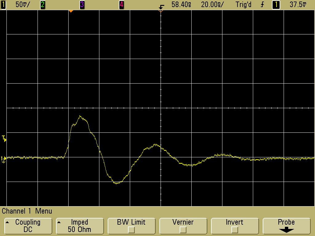
Figure 1. Measured Current Through a Protection Device on a PCB
(Vertical Scale = 50 mA/div, Horizontal Scale = 20 ns/div)
Abstract: Measuring voltage
stress on components on a PCB under ESD conditions can be difficult as
the ESD noise can inject error in the measurement. Often this error is
larger than the voltage of the stress to be measured. A method of
measuring voltage stress is discussed that has very high common mode
rejection and low ESD induced error.
Discussion: ESD induced error
makes accurately measuring voltage stresses on a PCB difficult. In
addition to high common mode noise, high amplitude time varying
electric and magnetic fields can introduce error in the measurement
loop formed by the voltage probe and the nodes to be measured unless
this loop is kept very small.
One way to accurately measure high frequency voltage stress is to
replace the component that is being stressed, such as an IC, with a TVS
or similar protector connected across the two nodes to be measured. In
series with the protector, form a loop as small as possible to insert a
current probe to measure the current through the protector.
As the ESD or other pulsed voltage stress is increased, an increase in current through the parasitic capacitance of the protector will be seen that follows the stress applied. When the breakdown voltage of the protector is reached, additional increase in current may be noted and the waveform will quickly show the current waveform as the stress is increased further for a protector that clamps to a specified value. For a protector that latches to nearly a short after turn-on, like an SCR, the current at the point of latching will be seen. Figure 1 shows the current through a protector that clamps to a specified voltage in a circuit with applied stress from a Fischer Custom Communications model TG-EFT high voltage pulser. The protector capacitance is helping form a resonant response with circuit inductance. The current waveform reaches a peak of about 80 mA.
In Figure 2, the stress is doubled and the peak current reaches about 150-160 mA, approximately increasing linearly with applied stress and keeping the same waveshape except the ringing frequency is slightly higher.
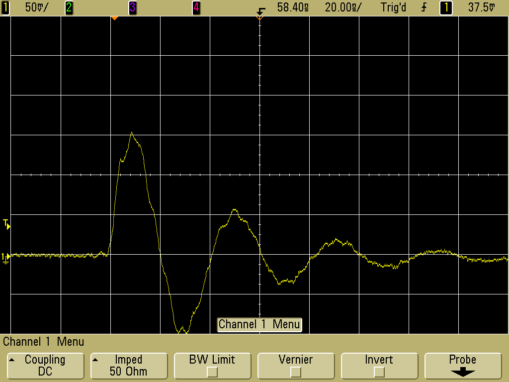
Figure 2. Measured Current Through Protection Device on a PCB at 2X Applied Stress
(Vertical Scale = 50 mA/div, Horizontal Scale = 20 ns/div)
For Figure 3, the stress is increased to 3X the value in Figure 1. Note that the waveshape is beginning to change although the peak current is about 3X of the current in Figure 1, about 230 mA.
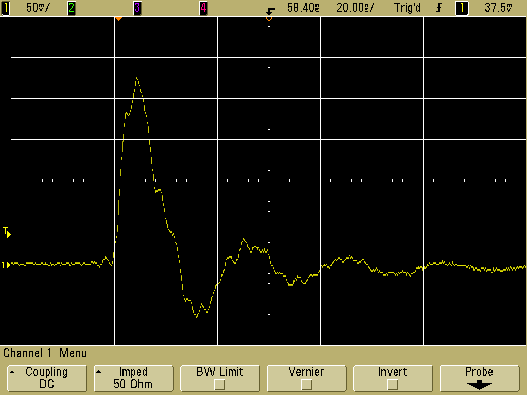
Figure 3. Measured Current Through Protection Device on a PCB at 3X Applied Stress
(Vertical Scale = 50 mA/div, Horizontal Scale = 20 ns/div)
In Figure 4, the stress is increased to 4X the value in Figure 1. Now the waveshape is definitely changed and is beginning to look like the current waveform I expect at this point in the circuit. The peak current is now almost 300 mA.
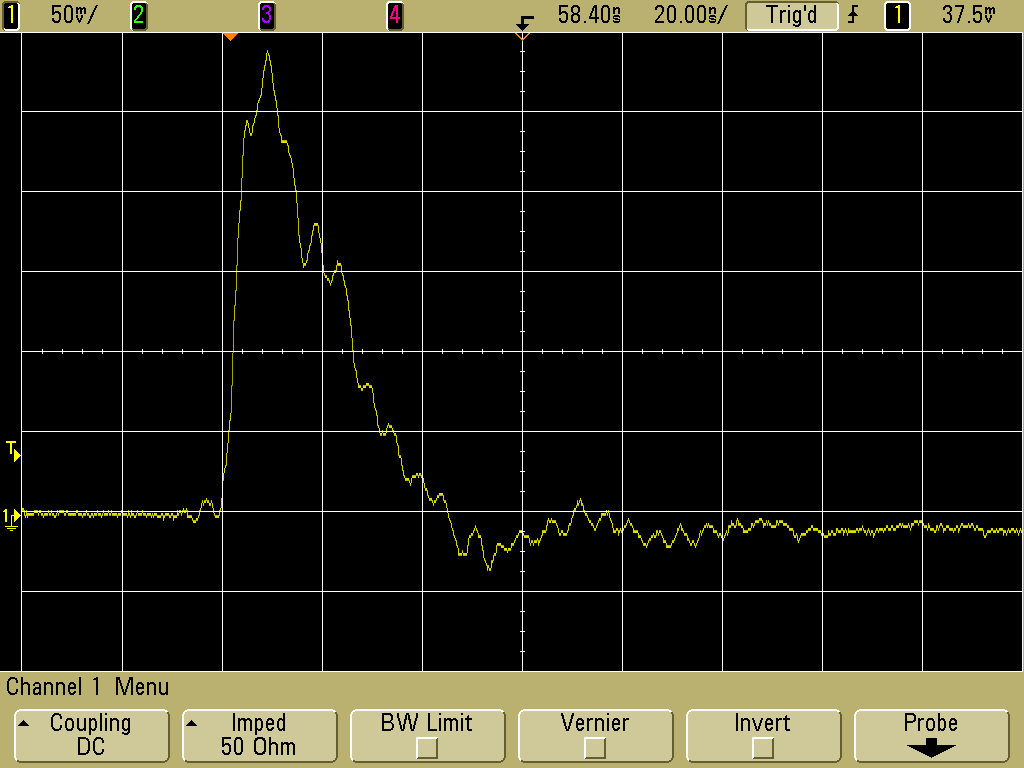
Figure 4. Measured Current Through Protection Device on a PCB at 4X Applied Stress
(Vertical Scale = 50 mA/div, Horizontal Scale = 20 ns/div)
The stress that just begins to breakdown the protector is that of
Figure 3 where the waveshape begins to change. Note that we are not
trying to accurately measure the current, so some electric field
response of the current probe is acceptable, we are looking for a
change in the waveshape of the current as the stress increases. The current probe should be as
small as possible so as to minimize the loop needed to insert it into the
circuit.
The lower capacitance the protector has before breakdown, the larger the difference in amplitude and waveshape will be noted at the point of breakdown. Also, if the capacitance of the protector is much larger than the original device it replaced, the capacitance may reduce the voltage across the protector resulting in a larger applied stress being required to breakdown the protector. This will result in measurement error that will understate the stress on the original device to be measured. In general, the lower capacitance the protector has the better, but for sure it should not be much larger than the original device it replaces in the circuit.
As the ESD or other pulsed voltage stress is increased, an increase in current through the parasitic capacitance of the protector will be seen that follows the stress applied. When the breakdown voltage of the protector is reached, additional increase in current may be noted and the waveform will quickly show the current waveform as the stress is increased further for a protector that clamps to a specified value. For a protector that latches to nearly a short after turn-on, like an SCR, the current at the point of latching will be seen. Figure 1 shows the current through a protector that clamps to a specified voltage in a circuit with applied stress from a Fischer Custom Communications model TG-EFT high voltage pulser. The protector capacitance is helping form a resonant response with circuit inductance. The current waveform reaches a peak of about 80 mA.
In Figure 2, the stress is doubled and the peak current reaches about 150-160 mA, approximately increasing linearly with applied stress and keeping the same waveshape except the ringing frequency is slightly higher.
Figure 2. Measured Current Through Protection Device on a PCB at 2X Applied Stress
(Vertical Scale = 50 mA/div, Horizontal Scale = 20 ns/div)
For Figure 3, the stress is increased to 3X the value in Figure 1. Note that the waveshape is beginning to change although the peak current is about 3X of the current in Figure 1, about 230 mA.
Figure 3. Measured Current Through Protection Device on a PCB at 3X Applied Stress
(Vertical Scale = 50 mA/div, Horizontal Scale = 20 ns/div)
In Figure 4, the stress is increased to 4X the value in Figure 1. Now the waveshape is definitely changed and is beginning to look like the current waveform I expect at this point in the circuit. The peak current is now almost 300 mA.
Figure 4. Measured Current Through Protection Device on a PCB at 4X Applied Stress
(Vertical Scale = 50 mA/div, Horizontal Scale = 20 ns/div)
The lower capacitance the protector has before breakdown, the larger the difference in amplitude and waveshape will be noted at the point of breakdown. Also, if the capacitance of the protector is much larger than the original device it replaced, the capacitance may reduce the voltage across the protector resulting in a larger applied stress being required to breakdown the protector. This will result in measurement error that will understate the stress on the original device to be measured. In general, the lower capacitance the protector has the better, but for sure it should not be much larger than the original device it replaces in the circuit.
Summary: Using a current
probe and a
protector connected in place of a device on a PCB to measure voltage stress on the device is a useful way
to minimize error from sources like ESD in the voltage stress
measurement. The capacitance of the protector used
should be minimized and be on the order of the original device
capactiance. The loop formed for the current probe should be as small
as possible.
Additional articles on this website related to this topic are:
- Current Probes, More Useful Than You Think (~170K)
- (1998 IEEE EMC Symposium paper)
- March 2011, Using High Frequency Measurement of ESD Current to Find Problems with an ESD Simulator
- Fischer Custom Communications F-65 Current Probe
- Fischer Custom Communications TG-EFT High Voltage Pulse Generator
- Agilent
DSO5054A oscilloscope
Need help with a design or additional training on technical subjects? Click on the image below to go to CircuitAdvisor.com, a new engineering resource for training, news, and fun.

If you like the information in this article and others on this website,
much more information is available in my courses. Click here
to see a listing of upcoming courses on design, measurement, and
troubleshooting of chips, circuits, and systems. Click here to see upcoming seminars in Newport Beach, CA.
Click here for a description of my latest seminar titled (now also available online as a WebEx seminar):
EMC
Lab Techniques for Designers
(How to find EMC problems and have some confidence your system will pass EMC testing while it is still in your lab).
(How to find EMC problems and have some confidence your system will pass EMC testing while it is still in your lab).
Home