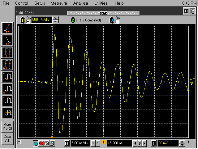
Figure 1. Voltage Drop Across a PCB's Very Short "Single Point Ground" Connection
(Vertical scale ~ 3V/div, Horizontal Scale = 5 ns/div)
Abstract: Single point
grounding is used successfully at power line frequencies and at DC to
keep currents from flowing in unintended paths within electronic
systems as well as in a few other applications. But, above a few MHz
and sometimes even at lower frequencies, single point grounding is not
achievable and significant currents and voltages will couple through
parasitic capacitance and inductance in the physical system. After a
discussion of some of the issues, a list of articles on this website
that address some of the problems that can result when single point
grounding is attempted in the presence of high frequency sources like
ESD and EMI are given.
Discussion: Figure 1 shows the
voltage induced across a short 1.5 cm long single point ground
connection to a circuit board when the underlying "chassis" is hit with
an ESD pulse. One would think that since the board is grounded in only
one point there should be no current in the ground connection. But even
a single picofarad of capacitance can allow Amperes of current to flow
that will produce significant voltage drop in circuits. Figure 1
appears in the
May 2002 Technical Tidbit on this website.
Consider a 2000 Volt change in potential across one pF of capacitance:
I = C dv/dt = 10-12F * 2000V/10-9s = 2 Amperes!
A 2000 Volt ESD event is below the threshold that most humans can perceive!
The
vertical scale in Figure 1 is about 3 Volts/div so the peak is about 10
Volts. And this across a short, thick wire about 1.5 cm long! So we see
that "single point ground" is not necessarily effective at high
frequencies. In my experience, ESD and EMC problems often result from
single point grounding systems unless very special attention is paid to
parasitic loops formed by inductance of conductors and capacitance
between conductors.
A list is included below the summary to four other Technical Tidbits on this website that discuss this topic.
Summary: Single
point grounding systems can cause significant problems at high
frequencies where many form of electrical stress, such as EFT, ESD, and
RF sources have significant energy. Only with very close attention to
the design can these high frequency problems be avoided in single point
grounding systems. Most of these systems I have seen have not been
successful in avoiding ESD and EMC problems.
I am writing this from my new office in Boulder City, NV!!! Still more
work to do on the move so the next few weeks will be very busy and the
May Technical Tidbit may be a little late as well. In addition, once
the move is complete, I expect to do morning 5 to 10 minute podcasts on
technical topics every morning I am in the office. These podcasts will
appear on the home page of
http://CircuitAdvisor.com by late morning each day except for days when I am not in the office.
Additional articles on this website related to this topic are:
Check
out my public seminar offering in Boulder City, NV. This is one of the
best seminar values around because the industry typical fee includes
more than just the seminar and lunch, but Lincoln Towne car airport
transportation in NV, lodging in the historic Bouder City Dam Hotel and
Museum, and breakfast and lunch each day. Click here for more details.
If you like the information in this article and others on this website,
much more information is available in my courses.
Click here
to see a listing of upcoming courses on design, measurement, and
troubleshooting of chips, circuits, and systems.
Click here to see upcoming seminars in Boulder City, NV.
|
Our office, laboratory, and classrooms are located in the
----------
Historic Boulder City Dam Hotel and Museum
1305 Arizona Street, Boulder City, Nevada 89005
Phone: (702) 293-3510
----------
Come
for a technical seminar, design review/troubleshooting, or just for a
visit and mix a little history of the Old West with your work!
|
|
|
|
Our Silicon Valley branch office and lab are located at
----------
NASA-Ames Research Center
RMV Technology Group
Bldg. 19, Suite 1073, M/S 19-46C
Moffett Field, CA 94035
|
Need help with a design or additional training on technical subjects? Click on the image below to go to
CircuitAdvisor.com, a new engineering resource for training, news, and
fun.
Click here for a description of my
latest seminar titled (now also available online as a WebEx seminar):
EMC
Lab Techniques for Designers
(How to find EMC problems and have some
confidence your system will pass EMC testing while it is still in your
lab).
Top of page
Home