(another use for the lowly paper clip)

Address: P. O. Box 1457, Los Gatos,
CA 95031
TEL:
800-323-3956/408-356-4186
FAX:
408-358-3799
Mobile: 408-858-4528
URL:
www.dsmith.org
Email: doug@dsmith.org
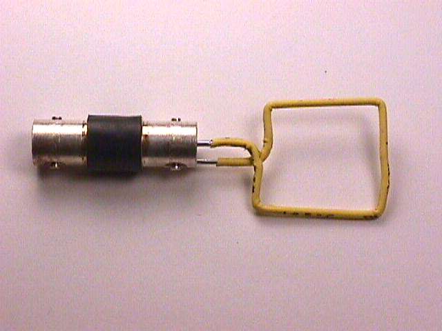
A square loop made from stiff wire (such as a bent paper clip) can be used as a "current probe" to trace currents flowing inside equipment and the resulting voltage drops due to EMI on the outside, such as an ESD event hitting the chassis of the equipment. For more information on the characteristics of such a loop, see the paper Signal and Noise Measurement Techniques Using Magnetic Field Probes on this site. The key to successful use is to reduce unwanted coupling of the interference into the loop and to prevent the presence of the loop from affecting the equipment under test (EUT) during the measurement.
For equipment that has a metal enclosure, skin effect can be used to keep EMI induced currents on the loop probe cable from getting into the equipment via the measurement setup. Figure 1 below shows a typical setup using a PC as an example.
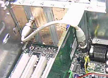
Figure 1. Loop Used to Sense Current on Printed Wiring Board
First, a BNC feedthrough connector is installed on one of the metal board slot covers used on PCs. The nearby gaps that can occur in the enclosure between the slot covers or board faceplates and the metal chassis are covered by copper tape. Skin effect will then keep currents induced on the loop cable on the outside of the enclosure.
Next, a short length of coax is connected from the BNC feedthrough connector to the pickup loop. The loop is positioned over the circuit board at the desired location. The loop is quite directional with a sharp null in output when current on the board is perpendicular to the loop and a broad peak in output when the current is flowing parallel to the side of the loop against the board.
To make sure the loop output is a result of current on the board being measured, a "null experiment" should be done. In this case, one such experiment is to suspend the loop a few inches above the board inside the enclosure. Since the mutual inductance between the loop and board falls off quickly as the loop is raised above the board, the output of the loop in this configuration is due mostly to pickup of fields in the enclosure leaking in through slots and seams. As long as this output is much smaller than when the loop is positioned on the board, its output when positioned against the board is due mostly to currents flowing in the board.
If the loop output is large when suspended away from the board and other metal, then these internal fields may in themselves be a problem. An output of 5 volts under this condition means other conductors inside the enclosure are picking up similar voltages, a likely problem.
Another "null experiment" is to replace the loop with a closed 50 Ohm termination at the end of the short internal coax cable. The output from this configuration represents the margin of error for any measurements by the loop.
Figure 2 shows the output of the loop in the position shown in Figure 1 when an ESD event was applied to the outside of the enclosure. The loop output represents a lower bound for the voltage drop on the ground plane between the two corners of the square probe. A discussion of this property is contained in the paper Signal and Noise Measurement Techniques Using Magnetic Field Probes on this site.
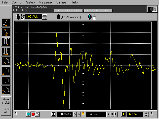
Figure 2. Loop Output From Board With Original Configuration
Note that the loop output attained a value of almost 4 volts peak. Since the loop is about an 2.5 cm on a side, the voltage drop on the board is at least 4 volts peak over a distance of 2.5 cm! An individual device would not see this much voltage per 2.5 cm of signal path because of mutual inductance between paths and the nearby ground/power plane. However, 4 plus volts of drop along 2.5 cm of a printed wiring board is not to be ignored.
Figure 3 shows the loop output from the same location when a grounding change was made on the board. Note that the peak voltage induced the loop is now about 1.6 volts, a significant reduction. In this particular case, this reduction was enough to eliminate an ESD induced problem.
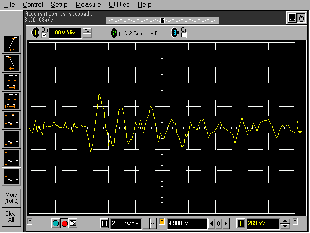
Figure 3. Loop Output From Board With Modified Grounding Arrangement
From the above data, one can conclude that not only is it possible to make measurements inside of equipment subjected to severe interference like ESD on the outside, but it can be done with relatively simple techniques.