Improving FET Probe Immunity to Unwanted Noise Pickup
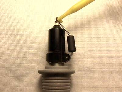
Figure 1. FET Probe Shorted by It's Ferrite Equipped Ground
Lead

Address: P. O. Box 1457, Los Gatos,
CA 95031
TEL:
800-323-3956/408-356-4186
FAX:
408-358-3799
Mobile: 408-858-4528
URL:
www.dsmith.org
Email: doug@dsmith.org

Figure 1. FET Probe Shorted by It's Ferrite Equipped Ground
Lead
High bandwidth, low capacitance FET probes often come with an accessory kit including various probing tips and ground connections. Accessory kits from several manufacturers include a ground connection with a ferrite bead, similar to that shown above. The purpose of the bead is to dampen the resonance of the probe input capacitance and the inductance of the measurement loop formed by the probe tip, ground connection, and circuit being measured.
However, the presence of the ferrite bead on the ground connection can cause the probe to become sensitive to outside interference that produces current flowing on the cable shield. Such currents can be the result of the radiation from an ESD event nearby or from logic noise currents flowing from the logic ground of the circuit being measured over the probe cable shield to the scope chassis. To test the sensitivity of the probe to such currents, one can short the probe to its ground connection as shown in Figure 1 and inject a signal on the probe tip. In this configuration, the probe is just measuring the voltage drop across the ground connection. I call this a null experiment because it shows how much error may be in the measurement because of ground currents and the result should be zero. In an actual measurement, the ground lead voltage drop is just added to the intended signal as far as the probed is concerned.
Figure 2 shows the result when the 5 volt square wave output of a HC240 gate running at the low frequency of about 30 MHz is applied to the shorted probe tip of Figure 1. The circuit ground of the HC240 is connected with a test clip to the scope chassis to provide a ground return for the signal in addition to stray capacitance. Figure 2 shows a signal of about 2 volts p-p from the shorted probe! This is the drop across the ground connection and ferrite bead in Figure 1 caused by the signal current flowing into the scope chassis.
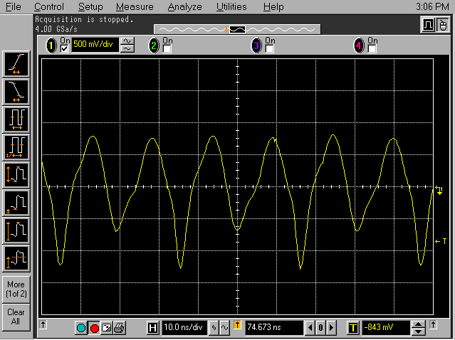
Figure 2. Probe Response to Logic Signal when Shorted with Bead
(Figure 1)
Figure 3 shows the ferrite bead ground lead replaced with a solid wire.
The same signal was applied to the probe tip with the result shown in Figure
4.
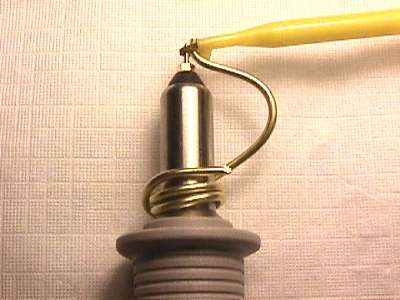
Figure 3. FET Probe Shorted with Short Wire
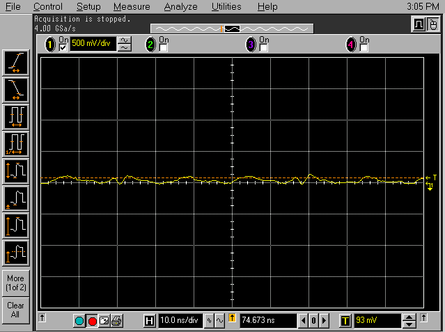
Figure 4. Probe Response to Logic Signal when Shorted with Short
Wire (Figure 3)
The original signal of about 2 volts p-p has been reduced to about 100 mV p-p! The reason is that the solid wire is a much lower impedance than the ferrite bead and its short ground wire. In fact, the presence of the ferrite bead raises the ground lead impedance such that the ground lead looks much longer than it actually is.
What does this mean to someone in the lab checking out a circuit? The presence of a ferrite bead in the ground lead, while improving probe response to the intended signal, increases the probe's response significantly to unwanted signals. For instance, a person touching an object across the room and generating an ESD event will cause the measurement to include a glitch due to the ESD event that is much larger than it would otherwise be. One might interpret the glitch as being actually in the circuit when in fact, it is not. This can be a real time burner in the development lab.
Other articles containing information on oscilloscope probe measurements on this site include:
The above waveforms were taken with an Agilent
Infinium 54845a oscilloscope.
More detailed information about this and other topics on this website is available from this site's new subscription service (to start this Fall) and seminars.