High Frequency MeasurementsWeb Page
Douglas C. Smith

 Address:  P. O. Box 1457, Los Gatos,CA 95031
 TEL:     800-323-3956/408-356-4186
 FAX:     408-358-3799
 Mobile:   408-858-4528
 URL:     www.dsmith.org
 Email:    doug@dsmith.org


Technical Tidbit - April 2003
Measurement and Interpretation of High Frequency Chip Noise
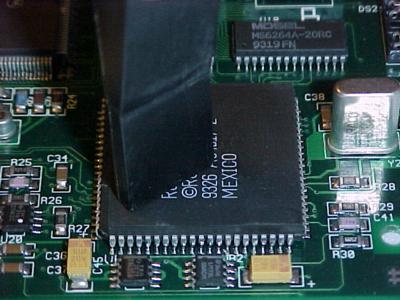
Loop on chip package for measurement
Figure 1. Square Loop Measurement of Chip Package Noise

Abstract: Voltage drops in chip packages can cause significantsignal integrity and EMC problems. The good news is that in many cases thesevoltages can be measured through mutual inductance. Measured results andtheir interpretation are discussed.

Discussion: Figure 1 shows a square shielded (shielding is not necessary for this measurement) loop positioned over a chip. Its output (Mdi/dt) isproportional to the voltage drop (Ldi/dt) across bonding wires and the lead frame of the chip package. In general, the loop output is a small fraction of the voltage drop in the package, about 25% in many cases. A detailed description of a method using the loop's output to diagnose chip package problems isgiven in the 1997 IEEE EMC Symposium paper on this site: A Method for TroubleshootingNoise Internal to an IC (~140K).In this method, a square loop is made so that one side of the loop spansthe distance from the center to the edge of the chip package.The loop is rotated 360 degrees looking for maximum noise while one corneris held at the package center. The paper includes many details omitted here.Interpretation of two typical cases, Figures 2 and 3 below is presented in this article.

Figure 2 shows a pulse recorded from a package similar in appearance and size to the one shown in Figure 1. Theimpulse shown in Figure 2 was an isolated pulse with very low duty cycle.Notice the peak value of about 125 mV. If the coupling of the voltage dropin the package to the loop is 25% (a typical value) then the voltage dropin the package is about 500 mV! This is enough to be cause for concern andits effect on the signal integrity of the chip should be investigated asoutlined in the paper referenced above. In general, the effects on signalintegrity of a loop output of more than 50 mV should be investigated.
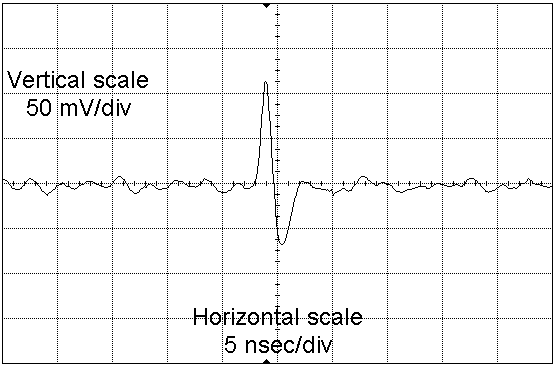
  Ldi/dt pulse from square loop
Figure 2.
Impulse Example

Since the loop output is Mdi/dt (where the di/dt is ofthe current flowing on the bonding wires and lead frame), the current waveformis proportional to the integral of Figure 2. The positive going pulse isthe rising edge and the negative pulse is the falling edge. For a squarewave, these two pulses will be separated. In the plot of Figure 2 though,they are adjacent. This means the current rises, in a little over a nanosecond,only to immediately fall with a slightly slower fall time. This is not likelya real signal but possibly the current pulse that occurs when a pull-up deviceoverlaps in time with a pull-down device resulting in cross conduction betweenpower and ground for a brief period. There are several other possibilities,such as conflict with another chip on a bus, that can result in such a currentwaveform.

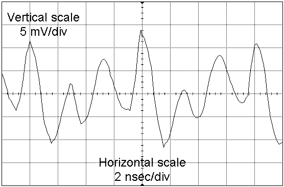
Figure 3, by contrast, shows a continuous signal from the loop. The fundamentalfrequency is about 125 MHz, but the interesting part is the easily seen thirdharmonic of about 375 MHz. The shape of the wave is similar to that shownin the April 2002 Technical Tidbit on this site, "Printed Wiring Board Couplingto a Nearby Metal Plane." In that article, the oscillator output excited a board resonance at the third harmonic of the oscillator frequency. In the present case, a board feature that resonates at 375 MHz may be excited. An example might be a path crossing a ground plane break or a misterminated transmission line. Another possibilityarises from circuitry and time delays internal to the device.

The difference between Figures 2 and 3 is that while the pulse in Figure2 may be a signal integrity problem because of its amplitude, the wave inFigure 3 may be an EMC emissions problem because it is continuous with significantenergy. Even though the peak amplitude is only about 13 mV, about one tenththe peak amplitude in Figure 2, the inductive voltage drop between the chipdie and one or more leads exiting the package is likely to be about 50 mV. Thiscould represent a noise plateau over the board ground plane driving all theleads of the chip with respect to the ground plane.

Considering that it only takes a couple of millivolts fed into an appropriate radiating structure to cause an emissions problem, every lead from this chipmay be a potential EMC problem waiting to happen. Even an output that ispulled low to drive an LED continuously, has the capability of deliveringsignificant energy to a radiating structure such as the board itself or connectedcables.

Ldi/dt CW signal from square loop
Figure 3.
CW (Continuous Wave) Example

Conclusion: Useful information can be obtained from relativelysimple measurement techniques. The data above clearly shows detection ofpossible signal integrity and EMC problems in a chip package by just lookingat the output from a square loop held against the chip package.

References:

 The data in the waveforms above was taken with an AgilentInfinium 54845a oscilloscope.

There is much that can be said about the above data andthis measurement technique that is not included here because of space limitations.More detailed information will be published on this topic and others in whitepapers on this website in the future. A demonstration of this effect has been recently added to my seminars.

Top of page
Home


Questions or suggestions? Contact me at doug@dsmith.org
Copyright © 2003 Douglas C. Smith