 High Frequency MeasurementsWeb Page
Douglas C. Smith Address: P. O. Box 1457, Los Gatos,CA 95031
TEL: 800-323-3956/408-356-4186
FAX: 408-358-3799
Mobile: 408-858-4528
URL: www.dsmith.org
Email: doug@dsmith.org
Technical Tidbit - July 2003
Measuring E-Field Coupled IC Chip Noise
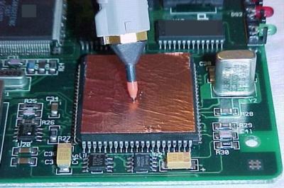
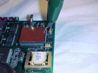
Figure 1. Chip E Field Noise Measurement
Abstract: Measuring noise coupled onto a copper foil patch appliedto a chip package can yield useful data. A method of measurement is suggestedand data presented. The data from such a measurement can be useful for design troubleshooting as well as EMC work.Uses related to reliable system operation and as well as conclusions for EMC compliance are presented.
Discussion: Figure 1 above shows a copper tape patch applied to achip package, A 0.8 pF low capacitance active probe (Agilent 1158a)is shown measuring the signal voltage on the patch. Such an arrangement can yield usefulinformation about the chip operation and its effect on nearby structures such as heat sinks.
Notice that there is no ground lead attached to the probe. The inputcapacitance of the probe is low enough that the capacitance of the probebody and the hand holding it forms the return path back to the board at highfrequencies. At lower frequencies, tens to hundreds of kHz, the scopeprobe shield through the scope chassis and earth ground forms the return(if the circuit has an earth ground connection). Thus, the ground referenceof the probe for frequencies in the megahertz range and above is an averageof the circuit board ground. The measurement is one of an average potentialfrom the chip surface and leads to an average ground potential on the board.The measurement, to a first order approximation, is made through the threepart capacitive divider of the capacitance of the chip and its bonding wiresto the copper tape, the probe input capacitance, and the capacitance fromthe probe back to the board. If a probe ground lead is used, its impedance becomes the third leg of the divider.
Ideally, the size of the copper patch should match the size of the chip,possibly covering bonding wires also. Too large a patch will act to slowthe observed risetimes or lower the signal amplitude for fast risetime signals.This is due to the added capacitance between the patch and the board as wellas the free space capacitance of the patch. This effect is described in theNovember 1999 Technical Tidbit, Transient Suppression Plane.
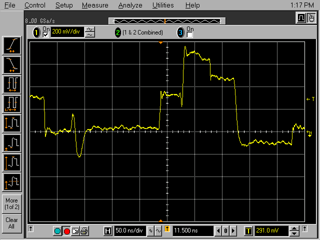
Figure 2 shows a measurement made in just such a way. The signal isalmost one volt peak-to-peak! This does not in itself mean there is a problem.Each step on the waveform means an area of the chip was raised in potential at that time, such as an address bus going from zeros to ones. The greater the area of the chip changing levels, the greater the step observed on the waveform.
One possible use for this display is to determine if chip operation has changed in a logical way as compared to another state. Another use couldbe to trigger a closer look at the chip and its surrounding circuits on theboard. A change in the waveform appearance could indicate a significant changein noise or EMC margins. For example, if an older chip is replaced by oneimplemented in a newer technology, a close look at the internal device risetimesmay be in order. A significantly faster risetime on internal signals, asindicated by this measurement, should be an indication that a closer inspectionof EMC and logic margins in the circuit is in order.
Consider the case of a heat sink attached to the chip package instead of copper tape. Something like the open circuitvoltage from this measurement is coupled onto the heat sink resulting in a current trying to returnto the circuit board. Such a current is at the root of many EMC complianceproblems.
Figure 2. Chip E Field Noise Waveform
(50 ns/div)
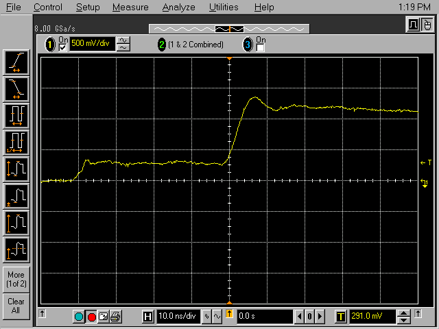
A handy use of this measurement technique is to determine internalrisetimes on the chip as mentioned earlier.Figure 3 shows a similar measurement, but at 10 ns/div instead of 50ns/div. One can see that the internal voltage risetimes on the chip are on the order2 to 5 ns. These times are relatively slow for this example becauseof the vintage of the chip being measured. Most modern chips will have risetimes much faster than this example.
Figure 3. Chip E Field Noise Waveform
(10 ns/div)
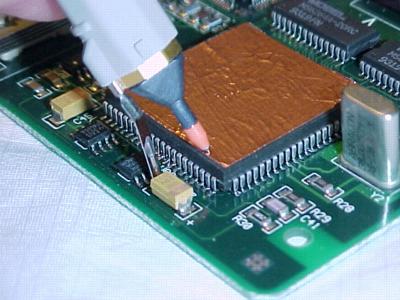
Figure 4 shows the use of a ground reference for the probe. The probe groundlead is touched to the board ground near the chip. Using such a probe groundreduces the loop area of the measurement considerably and can significantlyreduce noise pickup into the measurement from other sources, on and off theboard.
Figure 4. Chip E Field Noise Measurement Using Ground Lead
The use of a differential probe makes such a measurement even more accurate. Figure 5 shows a passive differential probe making the same measurement. Configurationssuch as Figure 4 and 5 can give an accurate representation of the open circuitvoltage induced on a heat sink. It is not difficult to come up with an estimatedsource impedance for this voltage. The capacitance between the chip and copperpatch or heat sink can result in an impedance at hundreds of megahertz andhigher on the order of a few hundred Ohms or less. This can result in currentson the order of milliamperes flowing through the heat sink and back intothe board whereas many EMC problems can be caused by tens of microamperesof current. It is easy to see why heat sink grounding is important.

Figure 5. Chip E Field Noise Measurement Using Passive Differential Probe
Summary and Conclusion: A measurement technique was presented thatcan yield useful information about chip operation, including logical operation,well as potential EMC problems. In particular, the importance of heatsink grounding is shown.
Equipment used in this article included:
Top of page
Home
Questions or suggestions? Contact me at doug@dsmith.orgCopyright © 2003 Douglas C. Smith