High Frequency Measurements Web Page
Douglas C. Smith

 page header graphic


Technical Tidbit - January 2014
Analog Designer's Notebook Part 2 - The Importance of Good Power Bypassing

Non-inverting opamp circuit with parasitic inductance

Figure 1.
Non-inverting Op Amp Circuit with Parasitic Inductance in Power Leads

Abstract: Power bypassing is more important than one would think for analog ICs like op amps. Even low frequency op amps need high quality power bypassing to prevent the op amp from breaking into oscillation at a much higher frequency than the unity gain bandwidth of the device. The reason for this and recommendations are presented.

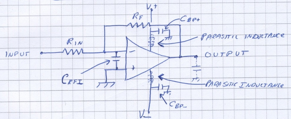
Figure 1 shows a typical inverting op amp circuit with parasitic inductance in the power connections. This inductance might be only a few tens of nanohenries and still cause problems, even for low frequency 1 MHz unity gain bandwidth op amps. Also shown in Figure 1 is the CRFI capacitor described in the November 2013 Technical Tidbit for increasing immunity to external EMI.

A problem occurs with inductance in the power leads because the inductance essentially adds another feedback loop from the output to the power pins, through the last stage or two of the op amp back to the output. The bandwidth of this feedback loop can be much higher than the bandwidth of the complete op amp. I have seen 1 MHz unity gain op amps oscillate at frequencies of over 20 MHz in response to inductance in the power leads!

This unwanted feedback loop occurs because driving current to the output causes drop across the power lead inductance which then feeds high frequency energy into the power pins (essentially another input). The op amp rejection of noise at the power pins is generally very low or non-existent at 20X the unity gain frequency of the op amp. Feeding capacitive loads can increase this effective feedback signal even further.

Many circuits utilizing 1 MHz unity gain op amps are constructed on two layer PCBs to save costs as they are perceived to be low frequency circuits, not needing the power and ground planes. Thus, the inductance between the op amp power pins and the nearest bypass capacitor is increased compared to multi-layer PCBs, aggravating the effect.

When designing op amp circuits, even low frequency ones, be sure to provide bypass capacitors right at the power pins, making as small a loop as possible between the + and - power pins.

Summary: Parasitic inductance in the power leads of op amp circuits can cause oscillation at frequencies well above the unity gain bandwidth of an op amp. Always provide bypass capacitor(s) between the power pins as close as possible to those pins to insure low parasitic inductance, even for low frequency circuits.


Check out my public seminar offering in Boulder City, NV. This is one of the best seminar values around because the industry typical fee includes more than just the seminar and lunch, but airport transportation in NV, lodging in the historic Boulder City Dam Hotel and Museum, and breakfast and lunch each day. Click here for more details.

The combination of the material presented, the venue, and the passionate presentation will likely make for the best technical short course/seminar you have ever taken! Didn't think a technical presentation can be passionate,? This one is. The result is this short course/seminar will likely be the most informative, practical, and FUN seminar you can attend.

If you like the information in this article and others on this website, much more information is available in my courses. Click here to see a listing of upcoming courses on design, measurement, and troubleshooting of chips, circuits, and systems. Click here to see upcoming seminars in Boulder City, NV.

Boulder Dam Hotel and Museum
Our office, laboratory, and classrooms are located in the
----------
Historic Boulder City Dam Hotel and Museum
1305 Arizona Street, Boulder City, Nevada 89005
Phone: (702) 293-3510
----------
Come for a technical seminar, design review/troubleshooting, or just for a visit and mix a little history of the Old West with your work!


Hangar One
Our Silicon Valley associate office and lab are located at
----------
NASA-Ames Research Center
RMV Technology Group
Bldg. 19, Suite 1073, M/S 19-46C
Moffett Field, CA  94035


Is your product failing ESD testing? Attend my webinar on sources of error in ESD testing. This webinar covers problems and mistakes often made in testing products for ESD compliance that can cause a good product to fail when it should pass. The webinar is given as both a scheduled event and on-demand. Contact me at doug@dsmith.org for more details. Don't let your product fail ESD testing unnecessarily. This webinar is an easy, cost effective solution.
Need help with a design or additional training on technical subjects? Click on the image below to go to CircuitAdvisor.com, an engineering resource for training, news, and fun.

CircuitAdvisor.com


Click here for a description of my latest seminar titled (now also available online as a WebEx seminar):

EMC Lab Techniques for Designers
(How to find EMC problems and have some confidence your system will pass EMC testing while it is still in your lab).


Top of page
Home

Questions or suggestions? Contact me at doug@dsmith.org
Copyright © 2013 Douglas C. Smith