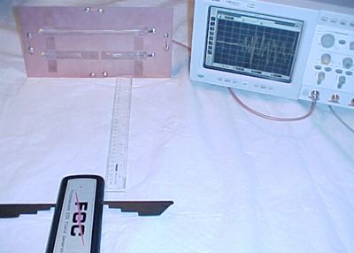
Figure 1. Test Setup to Measure Immunity of a Test Board

Address: P. O. Box 1457, Los Gatos,CA 95031
TEL: 800-323-3956/408-356-4186
FAX: 408-358-3799
Mobile: 408-858-4528
URL: www.dsmith.org
Email: doug@dsmith.org
Figure 1. Test Setup to Measure Immunity of a Test Board
Abstract: In 4 layer printed wiring boards, practical layouts require paths to cross from the top signal layer to the bottom signal layer. Pathsthat exist on both the top and bottom signal layers affect the emissionsand immunity characteristics of a circuit board. Results from a test of radiatedEMI are presented and discussed.
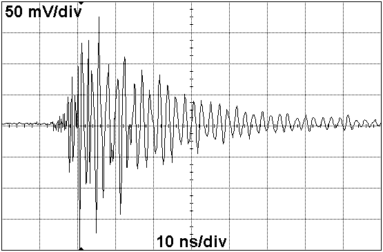
Figure 2 shows the voltage induced in the path that penetrated the copperplanes. A peak voltage of over 200 mV was recorded along with a ringing frequencybetween 400 and 500 MHz. The amplitude of the induced noise is a substantialfraction of the noise margin for some of today's fast logic. Potentially such a waveform could disrupt sensitive circuits..
Conclusion: The data shows that passing through copper planeson a circuit board can lead to lowered immunity to radiated and conducted EMI. In general,any board feature that disrupts the signal return path in a plane, will causelowered immunity to external EMI.
References:
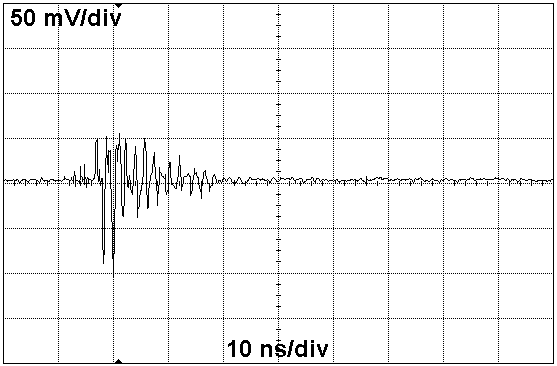
The data in the waveforms above was taken with an AgilentInfinium 54845a oscilloscope.
Shorting the edges of the planes together (directly or through bypasscapacitors) and other techniques are discussed, and shown as experiments, inmy seminars. These techniques can reduce the amount of EMI induced in boardfeatures such as diving through multiple ground or power planes.