
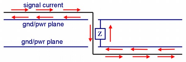
Figure 1. Signal Current Flow in a Layer Transition
Abstract: Printed wiring board, PWB, signal paths must
often change layers in a board stackup. Under some conditions this can
cause problems. An ESD example is used to illustrate the conditions
where changing layers can cause problems.
Figure 1 shows the case of a signal path that changes from the top layer of a four layer board to the bottom layer. While on the top and bottom layers, the signal current is matched by its image return current in the nearby ground or power plane. As the signal current changes layers from top to bottom an impairment that effects ESD performance can occur.
All signals form a loop, from source to load and back again to the source. It's often the "back again" part of the path that gets us into trouble, as we shall see for this specific case. The signal's returning current on the bottom of the bottom plane follows the signal to the top of the bottom plane, but it must pass through the interplane impedance, Z in Figure 1, to get to the bottom of the top plane from where it can follow the signal on to the top of the top plane.
One way to think of the impedance Z is to think of the the two planes as a two dimensional transmission line spreading out from the signal via. Bypass caps form low impedance "shorts" (although not all that good of a short at high enough frequencies where their inductance becomes important) and the edges of the board are generally unterminated "opens." These and other features cause reflections that contribute to an interplane impedance that varies significantly with frequency and can reach several Ohms at some frequencies for a four layer board with plane spacings on the order of 30 mils. Murphy's Law has it that one peak of this impedance will be at the third harmonic of your clock frequency!
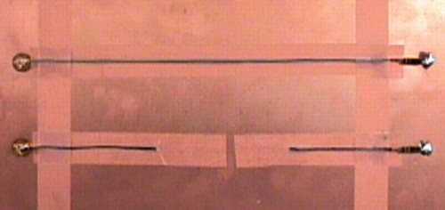
To evaluate this effect, I constructed the test board shown in Figure 2. Each signal trace is about 30 cm long. The traces are composed of one conductor of 100 Ohm twisted pair telephone wire. When taped to the ground plane, it forms a 50 Ohm path. The board is a double copper clad board and the whole assembly simulates a four layer PWB. The two copper planes are spaced about 30 mils apart and are shorted together by the SMA connectors on the left and at the load resistors on the right, four locations. One path stays on one side while the other penetrates the board and runs for about 10 cm on the other side.
The board was subjected to a 3 kV ESD contact discharge from an ESD simulator to the end of a one meter cable fastened to the plane shown in Figure 2 near the middle of the right edge while the middle of the left edge was connected to ground to drain charge from the board. Figure 3 shows the resulting apparent signal at the SMA connector for the top path of Figure 2 that stayed on the same side of the board. That signal was only about 400 mV.
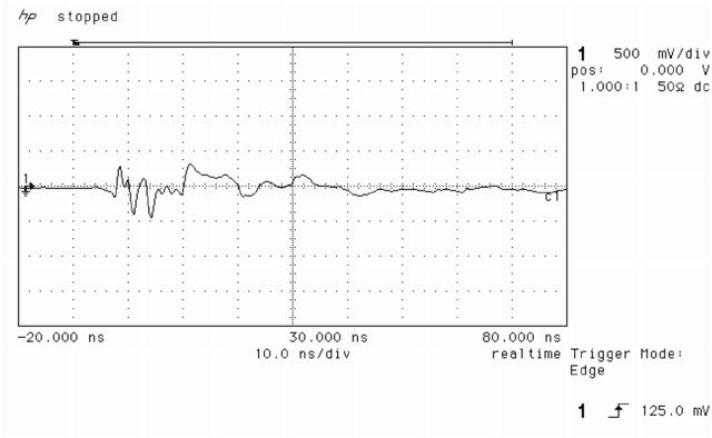
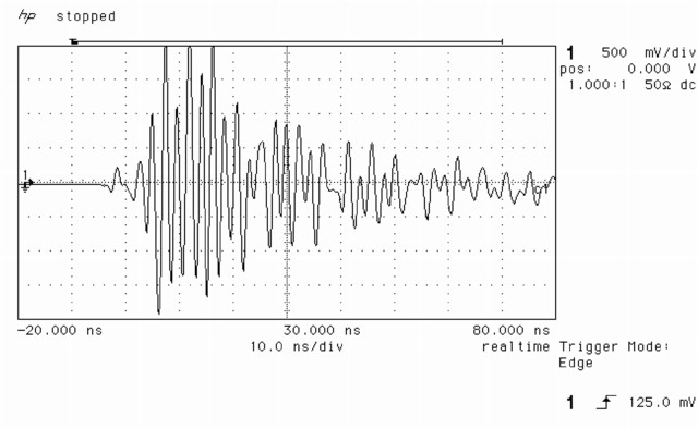
Figure 4 shows the apparent signal at the SMA connector of the lower path of Figure 2 that changed layers from the top to the bottom of the board and back. In this case, the peak signal at the SMA connector was over two volts peak and was oscillatory at the natural frequency of the assembly. This level would most certainly be a problem for most logic circuits. The increased noise in the lower path is due to the ESD
causing a voltage drop across the interplane impedance, Z, at each transition from one side of the board to the other. This voltage shows up in the signal/return loop and therefore appears at the SMA connector.
For cases where the interplane distance is much smaller than 30 mils, the interplane impedance will also generally be lower as well and the effect shown in Figure 4 will be smaller and less of a problem. The effect can also be minimized for a four layer board if critical signals transition from top to bottom of the board near existing (for low cost) bypass capacitors.
Summary: Transitioning between layers of a PWB can introduce significant impairment into a signal path. The larger the spacing between power and ground planes, the larger the effect. The example of a "four layer" PWB response to ESD shows one of the problems that can occur.
Discussion: Routing paths
in a PWB often requires the paths to change layers to accomplish the
layout. For a four layer PWB, this usually means changing from the top
layer to the bottom layer of the board, the two middle layers being
power and ground. A four layer board is especially problematical
because generally the separation between the power and ground layers is
relatively large, on the order of 30 to 40 mils, compared to boards
with six or more layers.
Figure 1 shows the case of a signal path that changes from the top layer of a four layer board to the bottom layer. While on the top and bottom layers, the signal current is matched by its image return current in the nearby ground or power plane. As the signal current changes layers from top to bottom an impairment that effects ESD performance can occur.
All signals form a loop, from source to load and back again to the source. It's often the "back again" part of the path that gets us into trouble, as we shall see for this specific case. The signal's returning current on the bottom of the bottom plane follows the signal to the top of the bottom plane, but it must pass through the interplane impedance, Z in Figure 1, to get to the bottom of the top plane from where it can follow the signal on to the top of the top plane.
One way to think of the impedance Z is to think of the the two planes as a two dimensional transmission line spreading out from the signal via. Bypass caps form low impedance "shorts" (although not all that good of a short at high enough frequencies where their inductance becomes important) and the edges of the board are generally unterminated "opens." These and other features cause reflections that contribute to an interplane impedance that varies significantly with frequency and can reach several Ohms at some frequencies for a four layer board with plane spacings on the order of 30 mils. Murphy's Law has it that one peak of this impedance will be at the third harmonic of your clock frequency!
To evaluate this effect, I constructed the test board shown in Figure 2. Each signal trace is about 30 cm long. The traces are composed of one conductor of 100 Ohm twisted pair telephone wire. When taped to the ground plane, it forms a 50 Ohm path. The board is a double copper clad board and the whole assembly simulates a four layer PWB. The two copper planes are spaced about 30 mils apart and are shorted together by the SMA connectors on the left and at the load resistors on the right, four locations. One path stays on one side while the other penetrates the board and runs for about 10 cm on the other side.
Figure 2. Test Board with Paths on a Single Layer and Two Layers
The board was subjected to a 3 kV ESD contact discharge from an ESD simulator to the end of a one meter cable fastened to the plane shown in Figure 2 near the middle of the right edge while the middle of the left edge was connected to ground to drain charge from the board. Figure 3 shows the resulting apparent signal at the SMA connector for the top path of Figure 2 that stayed on the same side of the board. That signal was only about 400 mV.
Figure 3. ESD Generated EMI to Path on One Layer
Figure 4 shows the apparent signal at the SMA connector of the lower path of Figure 2 that changed layers from the top to the bottom of the board and back. In this case, the peak signal at the SMA connector was over two volts peak and was oscillatory at the natural frequency of the assembly. This level would most certainly be a problem for most logic circuits. The increased noise in the lower path is due to the ESD
causing a voltage drop across the interplane impedance, Z, at each transition from one side of the board to the other. This voltage shows up in the signal/return loop and therefore appears at the SMA connector.
Figure 4. ESD Generated EMI to Path on Two Layers
For cases where the interplane distance is much smaller than 30 mils, the interplane impedance will also generally be lower as well and the effect shown in Figure 4 will be smaller and less of a problem. The effect can also be minimized for a four layer board if critical signals transition from top to bottom of the board near existing (for low cost) bypass capacitors.
Summary: Transitioning between layers of a PWB can introduce significant impairment into a signal path. The larger the spacing between power and ground planes, the larger the effect. The example of a "four layer" PWB response to ESD shows one of the problems that can occur.
Other articles on this website related to this topic are:
- Investigate System-Level ESD Problems
- Cover story for the November, 1999 issue of Test and Measurement World Magazine
- ESD Immunity in System Designs, System Field Experiences and Effects of PWB Layout (~950K)
- 2000 EOS/ESD Symposium paper
Available now for private on-site delivery and as a public seminar: my latest single day seminar titled: Failure Analysis and Prevention in Electronic Circuits (Design Troubleshooting for the Lab and Field).
 |
Check out my podcast containing mp3 format short tutorials, tech news and more! Just click on the microphone to see the listing
of free
audio programs. Content is added every week on technical topics so check back frequently. |
Home