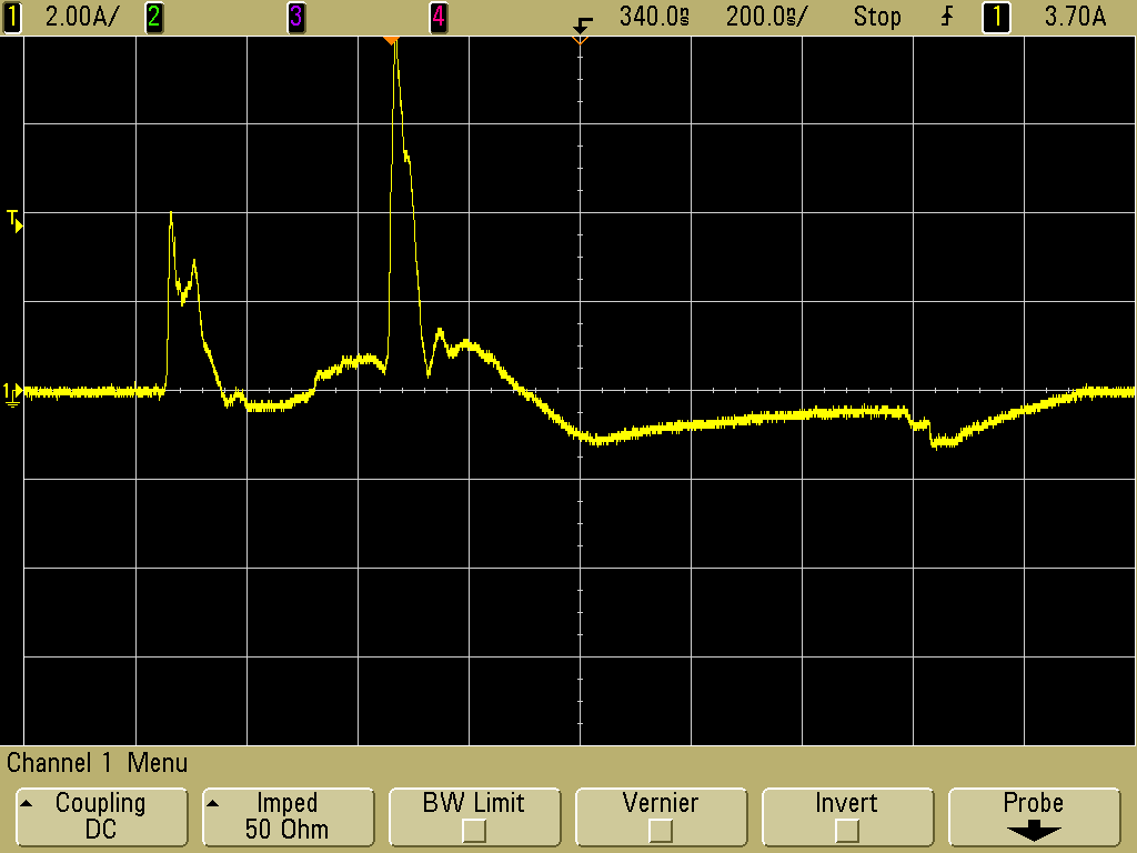
Figure 1. Current Waveform from ESD Simulator - Example 1
(Vertical = 2 Amp/div, Horizontal = 200 ns/div)
Abstract: Secondary discharges
formed in equipment in response to application of ESD, either simulated
or real, can cause significant problems ranging from upset to
actual damage of sensitive components. High frequency current
measurements are described that can be used to detect and evaluate the
severity of such secondary discharges. Examples are given.
Discussion: Figure 1 shows a
current induced in a system from an ESD simulator. One way to measure
such a current is shown in Figure 2 where
the ESD simulator is being discharged through a current probe (in this
case into horizontal coupling plane of an ESD test table, not a piece
of equipment). The current probe can also be located on system cables
either inside or outside the equipment enclosure. The time scale is
usually set to a few hundreds or nanoseconds so as to catch the
secondary discharge at the expense of detail on the high frequency
parts of the waveform. Since most current probes are AC coupled, the
area above the zero current line and below it must be equal over time.
This leads to the waveform apparently dipping below zero current when
it fact it may not be. Current dipping below zero on the right half of
Figure 1 is due at least partially to this effect.
Clearly there is a problem shown in Figure 1. After one impulse of current a second larger one occurs about 400 ns later. A secondary discharge, normally inside of the equipment under test, can have a greater impact on system operation than the original discharge because it is often closer to circuits and is sometimes more intense. On the second impulse in Figure 1, you can see a slow rise of current (possibly corona effects) followed by a fast rising edge of the breakdown. Subsequent discharges may look different and are likely to occur at somewhat different delays after the original discharge because of variations in the air discharge that forms the second impulse.
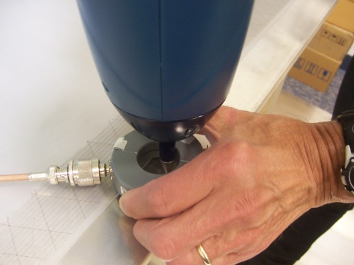
Figure 2. Current Waveform Measurement of ESD Simulator
Figure 3 contains another example , but in this case the secondary discharge looks much like the original discharge once the fast breakdown occurs. Effects like this can cause equipment to fail an ESD test where the fix is simply to find and eliminate the secondary discharge.
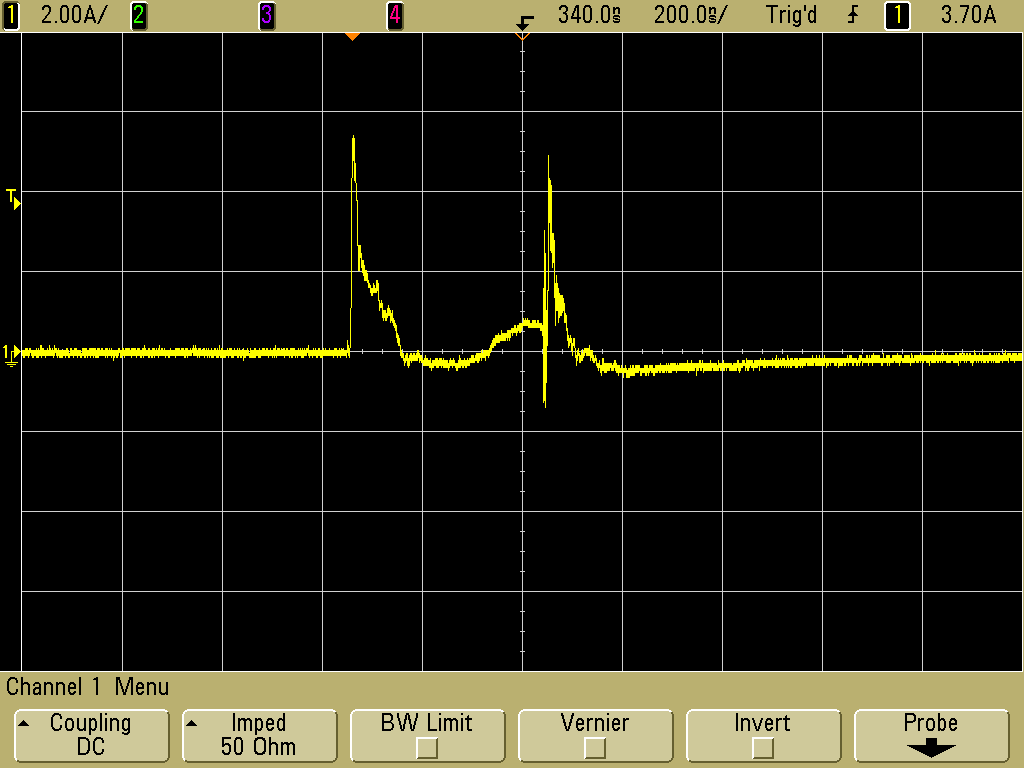
Figure 3. Current Waveform from ESD Simulator - Example 2
(Vertical = 2 Amp/div, Horizontal = 200 ns/div)
Clearly there is a problem shown in Figure 1. After one impulse of current a second larger one occurs about 400 ns later. A secondary discharge, normally inside of the equipment under test, can have a greater impact on system operation than the original discharge because it is often closer to circuits and is sometimes more intense. On the second impulse in Figure 1, you can see a slow rise of current (possibly corona effects) followed by a fast rising edge of the breakdown. Subsequent discharges may look different and are likely to occur at somewhat different delays after the original discharge because of variations in the air discharge that forms the second impulse.

Figure 2. Current Waveform Measurement of ESD Simulator
Figure 3 contains another example , but in this case the secondary discharge looks much like the original discharge once the fast breakdown occurs. Effects like this can cause equipment to fail an ESD test where the fix is simply to find and eliminate the secondary discharge.

Figure 3. Current Waveform from ESD Simulator - Example 2
(Vertical = 2 Amp/div, Horizontal = 200 ns/div)
The multiple discharges shown in
Figure 4 have very interesting characteristics. The initial discharge
is followed by a secondary one that is quite broad and a third one that
looks like the original discharge except it occurs 3 1/2 microseconds
later and is of opposite polarity! The current probe was located on the
tip of the ESD simulator to produce this waveform.
The equipment that resulted in the waveform in Figure 3 is very common. I took data on several examples of the equipment from different manufacturers and with two different ESD simulators of completely different designs. No doubt that a current waveform like this could be a real problem and warrants an article devoted entirely to this effect. I will publish this in the future either on this site or as a published paper on a new class of ESD problems for equipment in the field.
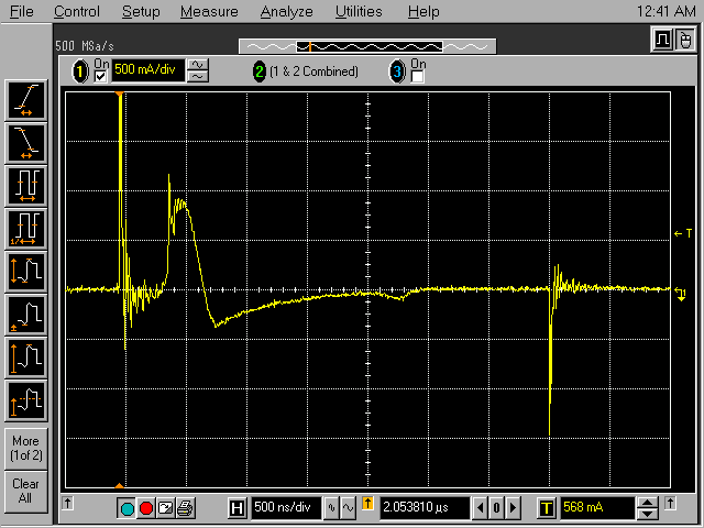
Figure 4. Current Waveform from ESD Simulator - Example 3
(Vertical = 1/2 Amp/div, Horizontal = 500 ns/div)
I would recommend using a good high frequency (flat response from 1 MHz or lower to 1 GHz or higher) current probe to measure both the discharge current of the ESD simulator and on system cables during ESD testing to find problems like those shown in Figures 1, 2, and 4 above. Events like these can explain a lot of problems in equipment (and with ESD simulators also!).
Summary:
Measuring ESD current during ESD testing can reveal the presence of
secondary discharges in equipment and allow the cause to be found and
fixed. Measuring the discharge current can also find problems with the
ESD simulator itself. This is especially important if you are using a
rented ESD simulator.
The equipment that resulted in the waveform in Figure 3 is very common. I took data on several examples of the equipment from different manufacturers and with two different ESD simulators of completely different designs. No doubt that a current waveform like this could be a real problem and warrants an article devoted entirely to this effect. I will publish this in the future either on this site or as a published paper on a new class of ESD problems for equipment in the field.

Figure 4. Current Waveform from ESD Simulator - Example 3
(Vertical = 1/2 Amp/div, Horizontal = 500 ns/div)
I would recommend using a good high frequency (flat response from 1 MHz or lower to 1 GHz or higher) current probe to measure both the discharge current of the ESD simulator and on system cables during ESD testing to find problems like those shown in Figures 1, 2, and 4 above. Events like these can explain a lot of problems in equipment (and with ESD simulators also!).
I would like to thank RMV Technology Group at NASA Ames Research Center for use of their facilities to generate the data for this Technical Tidbit.
Additional articles on this website related to this topic are:
- December 2010 Technical Tidbit, Comparing "IEC 61000-4-2 Compliant" ESD Simulators
- November 2010, Comparison of Current Waveforms from 150 Ohm and 330 Ohm Networks in an IEC 61000-4-2 Simulator
- Fischer Custom Communications F-65 Current Probe
- Agilent Infinium 54845a scope
- Agilent DSO5054A
- KeyTek MZ-15 ESD Simulator
- EM Test ESD 30N ESD Simulator
I would like to thank RMV Technology Group at NASA Ames Research Park for the use of their facilities to perform the tests for this article.
Need help with a design or additional training on technical subjects? Click on the image below to go to CircuitAdvisor.com, a new engineering resource for training, news, and fun.
Need help with a design or additional training on technical subjects? Click on the image below to go to CircuitAdvisor.com, a new engineering resource for training, news, and fun.
If you like the information in this article and others on this website,
much more information is available in my courses. Click here
to see a listing of upcoming courses on design, measurement, and
troubleshooting of chips, circuits, and systems. Click here to see upcoming seminars in Newport Beach, CA.
Click here for a description of my latest seminar titled (now also available online as a WebEx seminar):
EMC
Lab Techniques for Designers
(How to find EMC problems and have some confidence your system will pass EMC testing while it is still in your lab).
(How to find EMC problems and have some confidence your system will pass EMC testing while it is still in your lab).
Home
