
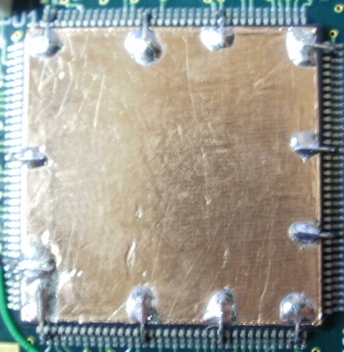
Figure 1. Example of an IC Package Shield Constructed of Copper Tape
Abstract: An IC package
"shield" made from copper foil tape can be used for troubleshooting a
number of problems including ground noise and some ESD problems.
Construction of such a shield and its applications are discussed.
Discussion: Figure 1 shows an example of a "shield" made of copper foil tape
which is connected to the ground pins of an IC package with short
wires. Sometimes the copper foil tape is not necessarily acting as a
shield but instead to improve the grounding under the IC such as in
single and two layer boards. Used either as a shield or to improve
grounding, such a structure can act as a troubleshooting aid for a
number of PCB problems. Examples of such problems include:
Construction of such a copper foil shield requires multiple low inductance connections to the board ground, often using the IC pins themselves. A flat pack, such as shown in Figure 1, has exposed leads which makes grounding of the foil very easy. The grounding connections must be very short, just a few millimeters, to work for ESD. Packages such as ball grid arrays that do not have exposed connections require the copper foil to be connected directly to the board ground which can be a challenge while trying to keep the connections short. The more connections and the shorter they are, the better.
Although not always a practical fix, construction of an IC package shield from copper foil tape can be a great troubleshooting aid on PCBs.
- Improving ground on single or two layer PCBs. Single and two layer PCBs are still quite common in electronic equipment, especially consumer equipment such as washing machines and other home appliances, DVD players and other consumer electronic equipment, switch mode power converters and supplies, and many other cost sensitive applications. Often on PCBs of this nature, significant ground noise voltages can be impressed between the ground pins of the IC device potentially causing operational problems. This is especially true of high frequency impulse noise due to ESD and EFT (electrical fast transient). Such noise can corrupt signals, cause latch-up, and even burn out ICs. Adding a copper tape plane on top of the IC package can improve the ground between the IC pins and fix problems. If a known problem is helped by this approach, some work is needed on the board layout.
- Reducing inductive and capacitive coupling from noise sources such as switch mode power converters and ESD to the IC package itself. In the case of ESD, sometimes the tip of an ESD simulator used for compliance testing can be close enough to an IC package to couple enough E and or H field noise directly into the IC package to cause problems. This is especially true for small products with a plastic housing where the tip of the simulator may be placed on a metallic feature (connector or even just a piece of decorative trim) very close to the IC package. Current generated by a time changing E field is given by:
i = C*dv/dt
where:
- i is the generated current
- C is the capacitance between the IC package and ESD simulator tip in this case, and
- dv/dt is the rate of change of voltage between the IC package and ESD simulator tip
Construction of such a copper foil shield requires multiple low inductance connections to the board ground, often using the IC pins themselves. A flat pack, such as shown in Figure 1, has exposed leads which makes grounding of the foil very easy. The grounding connections must be very short, just a few millimeters, to work for ESD. Packages such as ball grid arrays that do not have exposed connections require the copper foil to be connected directly to the board ground which can be a challenge while trying to keep the connections short. The more connections and the shorter they are, the better.
Although not always a practical fix, construction of an IC package shield from copper foil tape can be a great troubleshooting aid on PCBs.
Summary:
Construction of an IC package "shield" from copper foil tape and
multiple short wires can be a good troubleshooting aid for PCBs. The
shield is easiest to implement on ICs with exposed connections, such as
a flat pack, but can be successfully implemented on other package types
as well.
Additional articles on this website related to this topic are:
- September 2000, Copper Foil Tape, Anyone?
- December 2005, Applying Copper Foil Tape to a Metal Surface
Need help with a design or additional training on technical subjects? Click on the image below to go to CircuitAdvisor.com, a new engineering resource for training, news, and fun.

If you like the information in this article and others on this website,
much more information is available in my courses. Click here
to see a listing of upcoming courses on design, measurement, and
troubleshooting of chips, circuits, and systems. Click here to see upcoming seminars in Newport Beach, CA.
Click here for a description of my latest seminar titled (now also available online as a WebEx seminar):
EMC
Lab Techniques for Designers
(How to find EMC problems and have some confidence your system will pass EMC testing while it is still in your lab).
(How to find EMC problems and have some confidence your system will pass EMC testing while it is still in your lab).
Home