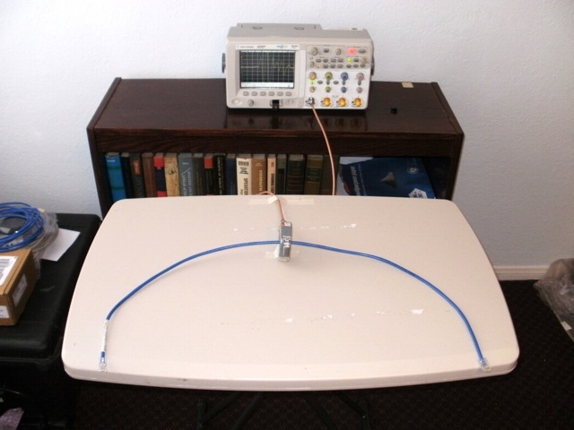
Discussion: Figure 1 shows the
test setup used for the experiment (the first one done in my new
Boulder City, NV facility) and Figure 2 shows a close-up of the test
table. A one meter Cat 5 Ethernet cable was used and the current in the
cable was measured by a Fischer F-65 current probe.
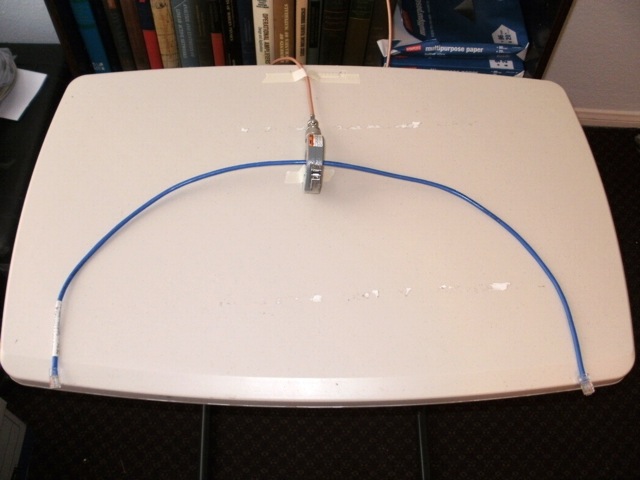
Figure 2. Test Setup for Measuring Induced Current in One Meter Cable
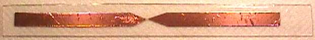
The ESD source is shown in Figure 3. It is described in
June 2001, A Static
Field Powered EMI Source on this site. ESD is generated in the very small gap between the points of the strips of
copper foil tape
when a charged object is brought close to one of the copper foil
strips. This is caused by electrons jumping across the gap due
attraction or repulsion by the applied electric field. Figure 4 shows a
charged strip of Teflon™being passed back and forth along the plastic
backing of the copper foil strips. This generates hundreds of ESD
events between the copper foil strips as electrons are chased back and
forth across the gap. I estimate the breakdown voltage of the gap to be
several hundred volts. The rising edge of the radiated field is on the
order of 200 to 300 ps.
Figure 3. Spark Gap EMI source for Experiment
Figure 4. Test Setup for Measuring Induced Current in One Meter Cable [1]
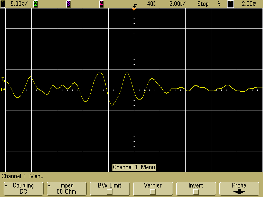
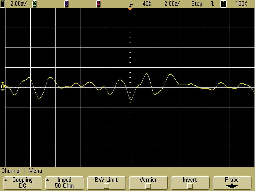
Three distances were used between the ESD events and the one meter
cable/current probe: 3 m, 1 m, and 30 cm. Figure 5 shows the induced
current at 3 m. The ringing in the waveform is due to the resonant
frequency of the copper foil strips (~500 MHz) and to some extent the
lower resonant frequency of the 1 m cable. Note the peak current of
about 17 mA. One of the most sensitive devices in use today are the
read heads in disk drives. They have an ESD Human Body damage threshold
of just a Volt or two (not thousands or even hundreds of volts, a few
volts)! [2] It takes just a milliamp or two for a nanosecond to
destroy the head. [2] Clearly, if such a head was not in a shielded
enclosure and connected to wires (for testing possibly), it could
easily be damaged from across the room. If one were to split the 1 m
cable in the middle to form a dipole, the two terminals at the middle
of the dipole would have enough voltage between them at a 70 Ohm source
impedance to damage a disk drive head from a voltage point of view as
well.
Figure 6 shows another typical current waveform generated showing
greater than 20 mA flowing in the 1m cable, an even worse case. This is
enough to damage even the older GMR heads of 15 years ago. Those heads
were damaged by 20 mA flowing for a nanosecond.
Figure 5. Discharge at 3 m From Cable and Current Probe - #1
(Vertical scale ~ 5 mA/div, Horizontal Scale = 2 ns/div)
Figure 6. Discharge at 3 m From Cable and Current Probe - #2
(Vertical scale ~ 5 mA/div, Horizontal Scale = 2 ns/div)
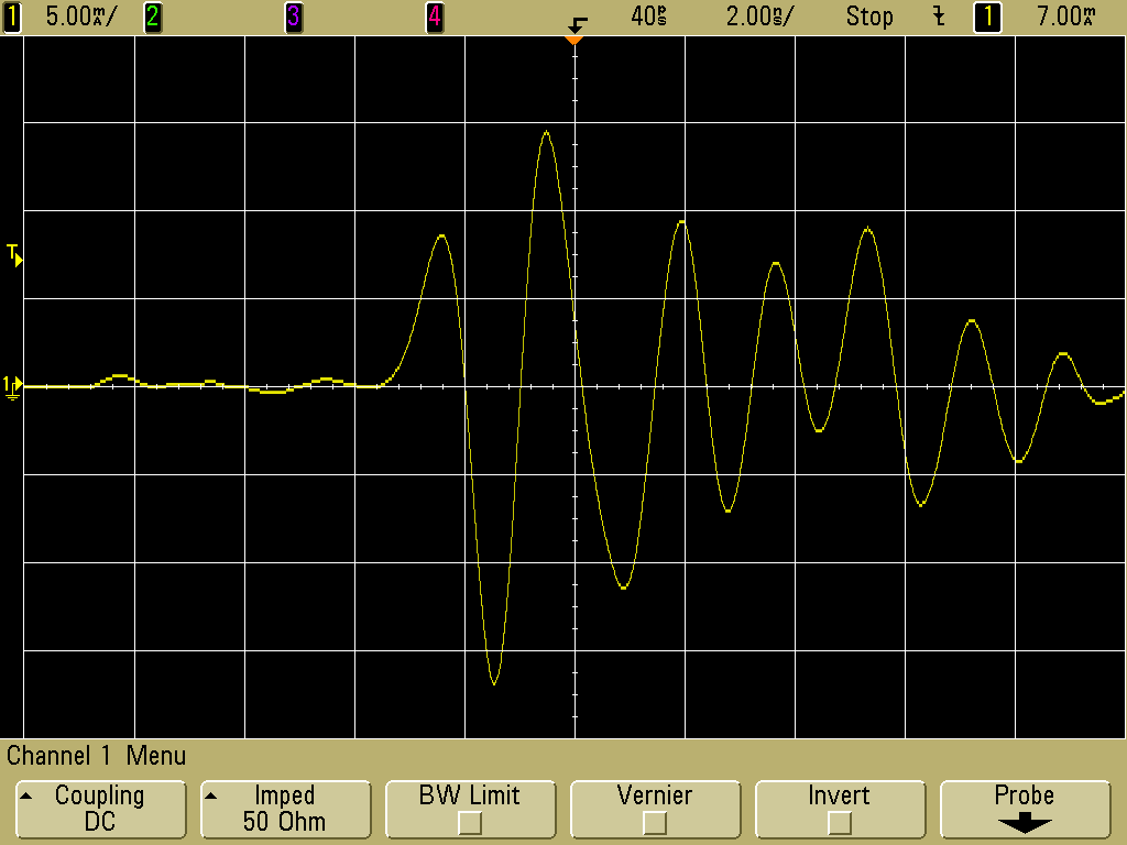
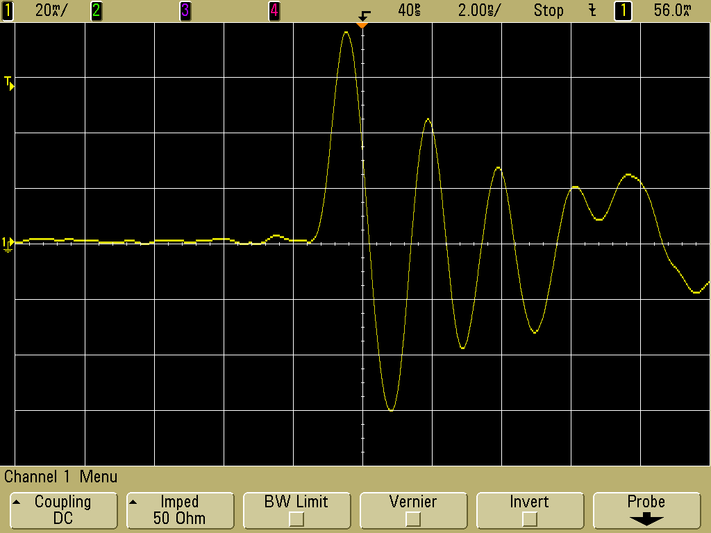
Figures 7 and 8 show the measured currents at a distance of one meter
from the ESD events. The peak current for this distance was over 40 mA!
Figure 7. Discharge at 1 m From Cable and Current Probe - #1
(Vertical scale ~ 10 mA/div, Horizontal Scale = 2 ns/div)
Figure 8. Discharge at 1 m From Cable and Current Probe - #2
(Vertical scale ~ 10 mA/div, Horizontal Scale = 2 ns/div)
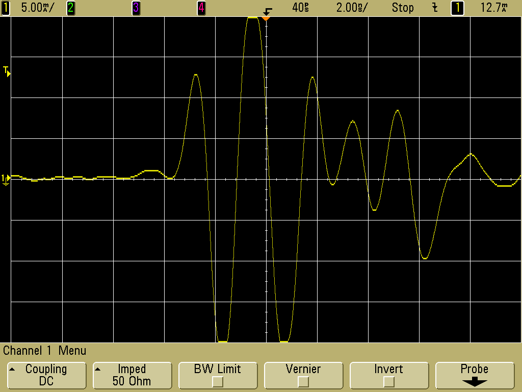
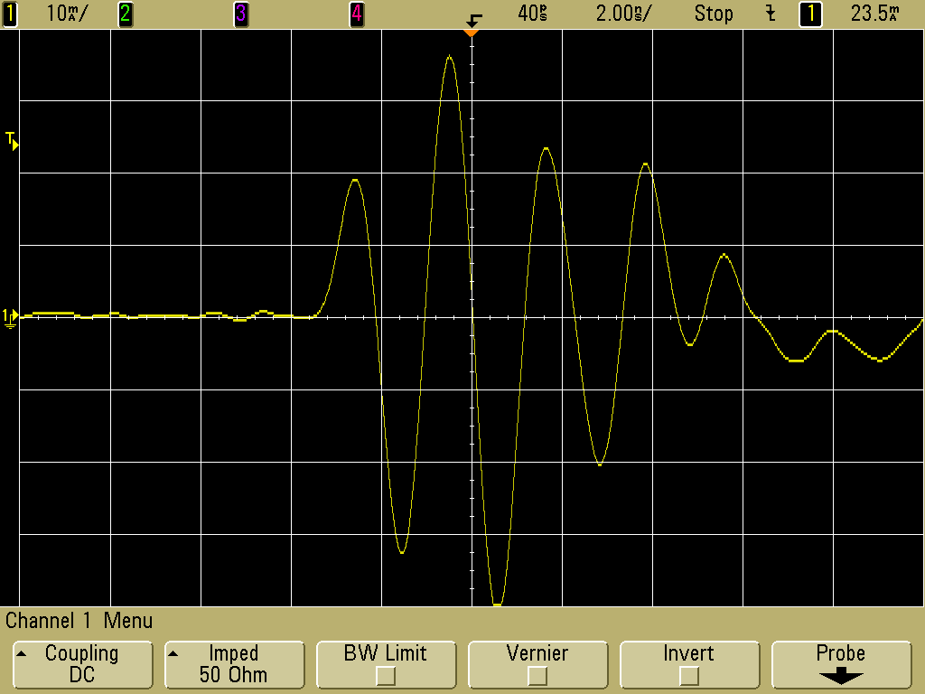
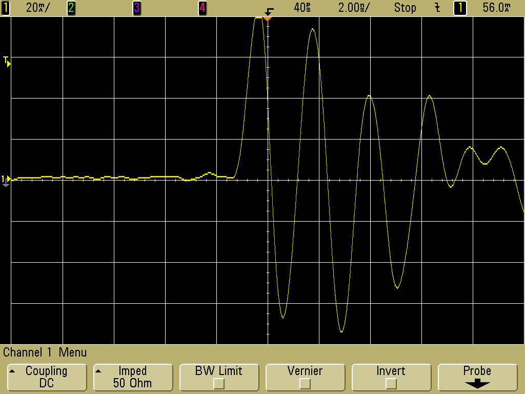
Figures 9 and 10 show the measured currents at 30 cm. The peak current
is greater than 80 mA in Figure 10. The induced current from a remote
discharge having more energy could be much larger than this.
Figure 9. Discharge at 30 cm From Cable and Current Probe - #1
(Vertical scale ~ 20 mA/div, Horizontal Scale = 2 ns/div)
Figure 10. Discharge at 30 cm From Cable and Current Probe - #2
(Vertical scale ~ 20 mA/div, Horizontal Scale = 2 ns/div)
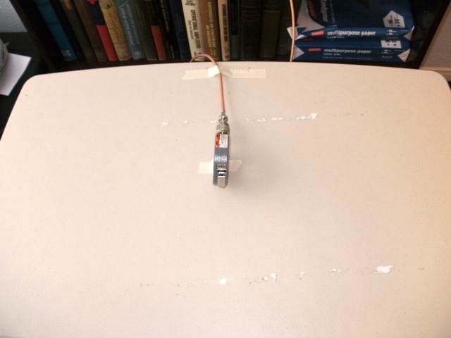
In order to check for EMI from the ESD directly into the measurement, a
null experiment, the 1 m cable was removed from the current probe,
leaving the probe alone on the table as shown in Figure 11. ESD was
generated as before at about 30 cm and the results are shown in Figure
12 and 13. The peak reading recorded was about 4 mA. This represents
less than 5% error compared to the greater than 80 mA displayed in
Figure 10, an acceptable amount of error.
Figure 11. Null Experiment Discharge at 30 cm From Current Probe
Figure 11. Null Experiment Discharge at 30 cm From Current Probe - #1
(Vertical scale ~ 5 mA/div, Horizontal Scale = 2 ns/div)
Figure 12. Null Experiment Discharge at 30 cm From Current Probe - #2
(Vertical scale ~ 2 mA/div, Horizontal Scale = 2 ns/div)
There
are many devices very sensitive to ESD in use today. They carry an ESD
damage threshold rating of Class 0, less than 50 volts Human Body
Model. For such devices, especially the very sensitive devices like
modern disk drive heads, damage from ESD remote from the device is a
real possibility. ESD must be controlled not just at the component, but
in the nearby environment as well.
Summary: Devices
have gotten so sensitive that we now have to worry about ESD damage
from ESD events that may be several meters from the device in question.
The implication for ESD control is obvious, much stricter ESD controls
must be employed and not just at the workstation where the device is
handled. ESD must be controlled for a distance of several meters from
the sensitive device. This is especially true for disk drive read heads.
I am writing this from my new office in Boulder City, NV!!! Soon I expect to do morning 5 to 10 minute podcasts on
technical topics every morning I am in the office. These podcasts will
appear on the home page of
http://CircuitAdvisor.com by late morning each day except for days when I am not in the office.
[1] Thanks to my youngest son, David, for generating the ESD events
while I measured the result. He just finished four years in the Army in
electronic repair and will be going into EE or CE towards the end of
this year.
[2] From a discussion with Al Wallash, HGST, a Western Digital Company, about published data.
Additional articles on this website related to this topic are:
Equipment used in this Technical Tidbit:
- Fischer Custom Communications F-65 Current Probe
- Agilent
DSO5054A