
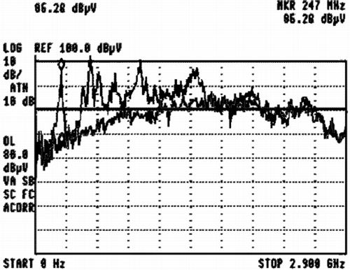
Figure 1. Relative Emissions for Two Paths
(one passes from top to bottom layer (plot with peaks) and the other stays on one side)
Abstract: Printed wiring board, PWB, signal paths must
often change layers in a board stackup. Under some conditions this can
cause problems. An emissions example is used to illustrate the conditions
where changing layers can cause problems.
Figure 1 depicts emissions from the board shown in Figure 2, the same one used for an ESD example in last month's April 2006 Technical Tidbit, The paths on the board are about 30 cm in length. One stays on the same side of the board while the other passes through to the other side for about 10 cm. The two metal planes are about 30 mils apart and are shorted together by the SMA connectors and at the 47 Ohm load resistors. The paths are made of one insulated conductor made from 24 gauge twisted pair telephone wire. Since the original cable had a differential impedance of 100 Ohms, one of the wires taped down to a copper plane will have a characteristic impedance of 50 Ohms with respect to the metal plane.
The data for Figure 1 was generated by exciting one path with the tracking generator of a spectrum analyzer and attaching an emissions measurement antenna to the input of the spectrum analyzer. The antenna had reasonable antenna factors up to about 3 GHz. Figure 3 shows the board sitting on a cardboard box in an EMC chamber. The coax on the left comes from the tracking generator and the one meter white wire on the right is just hanging off the box connected to one of the board planes by an alligator clip. It was included in case signal voltage on the planes might cause attached cables to radiate. The coaxial cable shield and the added wire form something of a dipole, albeit an asymmetric one.
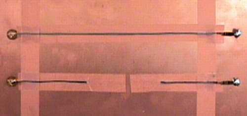
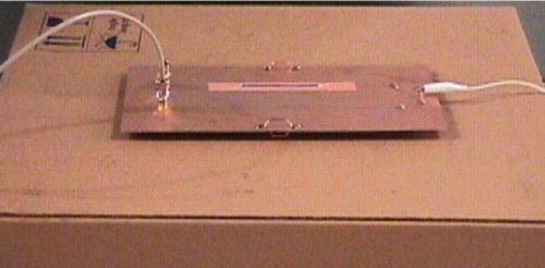
Figure 1 was generated by overlaying emissions data from the two paths shown in Figure 2. The plots cover the frequency range from near DC up to 2.9 GHz. The absolute magnitude of the plots is not important. It depends on the output power of the tracking generator, but the comparison between the two plots is striking. The lower trace resulted from the path that stayed on one side of the board while the upper trace, showing pronounced peaks, resulted when the path that passed through the board was energized. Note that the first peak at 247 MHz is nearly 30 dB above the emissions at that frequency from the path that stayed on the same side of the board.
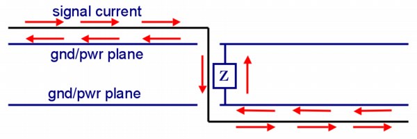
Figure 4 shows the signal currents in the wire and planes as the signal passes through the boards. As described in detail in last month's April 2006 Technical Tidbit, a complex interplane impedance, Z, appears in the signal return path as it passes between the planes. The voltage generated across this impedance by the signal current as well as other effects contribute to the emissions shown in Figure 1.
For cases where the interplane distance is much smaller than 30 mils, the interplane impedance will also generally be lower as well and the effect shown in Figure 1 will be smaller and less of a problem. The effect can also be minimized for a four layer board if critical signals transition from the top layer to the bottom layer of the board near existing (for low cost) bypass capacitors.
Summary: Transitioning between layers of a PWB can introduce significant impairment into a signal path. The larger the spacing between power and ground planes, the larger the effect. The example of a "four layer" PWB emissions profile shows one of the problems that can occur.
Discussion: Routing paths
in a PWB often requires the paths to change layers to accomplish the
layout. For a four layer PWB, this usually means changing from the top
layer to the bottom layer of the board, the two middle layers being
power and ground. A four layer board is especially problematical
because generally the separation between the power and ground layers is
relatively large, on the order of 30 to 40 mils, compared to boards
with six or more layers.
Figure 1 depicts emissions from the board shown in Figure 2, the same one used for an ESD example in last month's April 2006 Technical Tidbit, The paths on the board are about 30 cm in length. One stays on the same side of the board while the other passes through to the other side for about 10 cm. The two metal planes are about 30 mils apart and are shorted together by the SMA connectors and at the 47 Ohm load resistors. The paths are made of one insulated conductor made from 24 gauge twisted pair telephone wire. Since the original cable had a differential impedance of 100 Ohms, one of the wires taped down to a copper plane will have a characteristic impedance of 50 Ohms with respect to the metal plane.
The data for Figure 1 was generated by exciting one path with the tracking generator of a spectrum analyzer and attaching an emissions measurement antenna to the input of the spectrum analyzer. The antenna had reasonable antenna factors up to about 3 GHz. Figure 3 shows the board sitting on a cardboard box in an EMC chamber. The coax on the left comes from the tracking generator and the one meter white wire on the right is just hanging off the box connected to one of the board planes by an alligator clip. It was included in case signal voltage on the planes might cause attached cables to radiate. The coaxial cable shield and the added wire form something of a dipole, albeit an asymmetric one.
Figure 2. Test Board with Paths on a Single Layer and Two Layers
Figure 3. Emissions Test Setup
Figure 1 was generated by overlaying emissions data from the two paths shown in Figure 2. The plots cover the frequency range from near DC up to 2.9 GHz. The absolute magnitude of the plots is not important. It depends on the output power of the tracking generator, but the comparison between the two plots is striking. The lower trace resulted from the path that stayed on one side of the board while the upper trace, showing pronounced peaks, resulted when the path that passed through the board was energized. Note that the first peak at 247 MHz is nearly 30 dB above the emissions at that frequency from the path that stayed on the same side of the board.
Figure 4 shows the signal currents in the wire and planes as the signal passes through the boards. As described in detail in last month's April 2006 Technical Tidbit, a complex interplane impedance, Z, appears in the signal return path as it passes between the planes. The voltage generated across this impedance by the signal current as well as other effects contribute to the emissions shown in Figure 1.
Figure 4. Signal Paths Through a Via
For cases where the interplane distance is much smaller than 30 mils, the interplane impedance will also generally be lower as well and the effect shown in Figure 1 will be smaller and less of a problem. The effect can also be minimized for a four layer board if critical signals transition from the top layer to the bottom layer of the board near existing (for low cost) bypass capacitors.
Summary: Transitioning between layers of a PWB can introduce significant impairment into a signal path. The larger the spacing between power and ground planes, the larger the effect. The example of a "four layer" PWB emissions profile shows one of the problems that can occur.
Other articles on this website related to this topic are:
- February 2005, Crossing Ground Plane Breaks - Part 5, Common Mode Currents and Emissions
- March 2006, Predicting Cable Emissions from Common Mode Current
Available now for private on-site delivery and as a public seminar: my latest single day seminar titled: Failure Analysis and Prevention in Electronic Circuits (Design Troubleshooting for the Lab and Field).
 |
Check out my podcast containing mp3 format short tutorials, tech news and more! Just click on the microphone to see the listing
of free
audio programs. Content is added every week on technical topics so check back frequently. |
Home