Abstract: Tackling radiated
and conducted immunity problems can be difficult because of the high
cost of the equipment and chamber normally used to perform these tests.
An inexpensive test bench setup that can effectively find radiated and
conducted immunity problems is presented.
Finding and fixing radiated immunity
problems can be difficult because the chambers and associated equipment
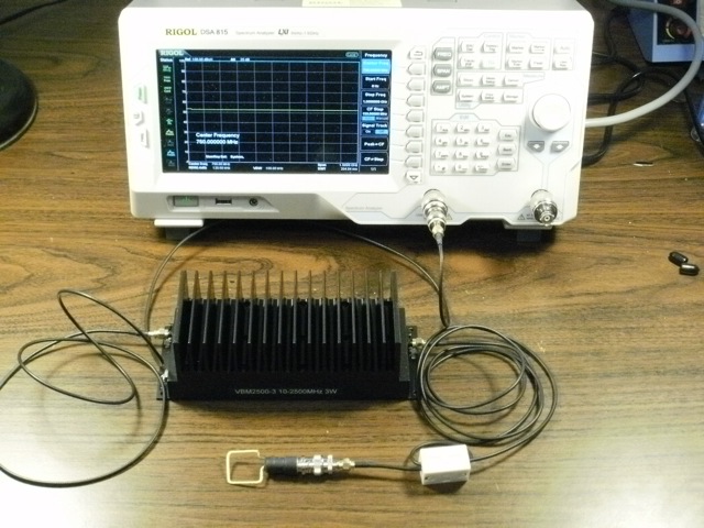
are expensive and generally not available in the design lab. Figure 1
shows a test setup that is useful for debugging radiated and conducted immunity
issues right on the design bench. Shown in the picture are a Vectawave
VBM2500-3 three Watt RF amplifier, a Rigol DSA815 spectrum analyzer (used for its
tracking generator in this test), and a homemade square one inch loop
driven by the VBM2500-3 amplifier (links to the equipment are listed at the end of
this Technical Tidbit).
With this equipment, an engineer can find locations in equipment that
respond to RF signals in an unwanted way. For an RF output of about one
Watt, voltages and currents can be induced in equipment that are
comparable to that of a 100 V/m RF field (lots of assumptions here),
but just locally near the side of the loop held nearest the circuit.
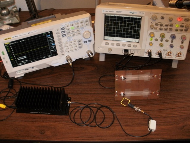
To
see the kind of signals that can be produced, Figure 2 shows the
overall test setup including an Agilent DSO5054A oscilloscope and a
homemade circuit board with a path crossing a 5 cm ground plane break
(a no-no in board design). The path runs from a BNC connector to a 47
Ohm load resistor to terminate the approximately 50 Ohm path. The BNC
connector on the board is connected to the channel one input on the
scope.
The
tracking generator in the spectrum analyzer is set to 400 MHz and is
driving the input of the amplifier at a level of about -7 dBm. The
amplifier has a gain of about 38 dB so the power output (if into a 50
Ohm load) is about 31 dBm, a little over a Watt.
Figure 2. Test Setup to Investigate RF Induction into a PCB with a Ground Plane Break
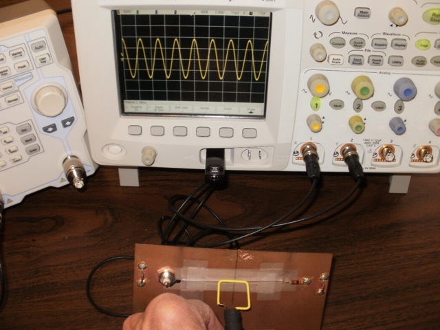
In Figure 3, the square wire loop (fancy term: magnetic field probe) is
being held up to the path crossing the ground plane break and the
resulting plot on the oscilloscope can be seen. Figure 4 shows the scope trace in
detail.
Figure 3. RF Signal Injection Into Path on the Test Board
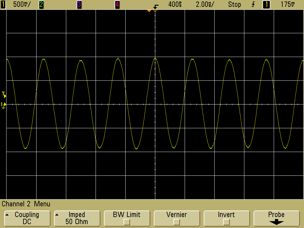
Figure 4. Resulting Signal Injected Into the Signal Path
In Figure 4, we can see that about one Volt peak of RF at 400 MHz was
induced in the path for an output from the amplifier of about 31 dBm, a little over one Watt. A lot of that power is
reflected back to the amplifier from the loop, but enough is injected
into the circuit to simulate the effect a significant external RF field.
This method can be used to inject energy into electrical resonances in
a system and other circuits as well, to find parts of a system that might be the
cause of a radiated immunity problem. This method can also be used to
find problem areas in a system experiencing conducted immunity problems
as well.
Summary: Using an
inexpensive RF source, a small power amplifier, and loop probe, an
engineer can find sensitive parts of a system that could cause a
radiated or conducted immunity problem. Using this method of generating
local fields, troubleshooting a piece of equipment can be done right on
the development table, a much more convenient place to work than an EMC
test lab.
Technical Tidbits on this site related to this article:
Equipment used in this Technical Tidbit: