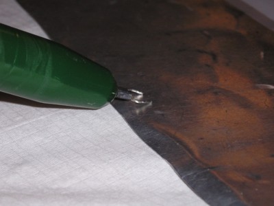
Figure 1. Passive Differential Probe Shorted on Metal Plate - a Null Experiment
Abstract: A passive
differential probe can be very useful for making voltage measurements
in the presence of severe interference such as nearby ESD. In such a situation,
active differential probes cannot be used because of common mode input
voltage limitations. Data is presented to show typical effectiveness of
a passive differential probe.
Discussion: Figure 1 shows two probe tips of a passive differential probe connected to the same metal sheet as used in the November 2006 Technical Tidbit, Measuring Signals in the Presence of Severe EMI - Part 1, How Not to Do It.
The metal sheet is about 40 cm by 30 cm and is meant to simulate the ground plane of a
large circuit board that a probe might be connected to. In the November
article, the data presented showed that either single ended scope
probes or using two separate probes and
channel subtraction in the scope does not work well if severe EMI is
present.
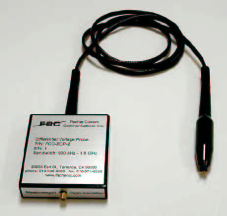
A true differential measurement holds the promise of rejecting EMI, but modern active differential probes can only withstand a common mode voltage of a few Volts. The prototype passive differential probe in Figure 1 is made from passive linear components and as such does not have the low common mode voltage range of high bandwidth (above one GHz) active probes. Click here for a description (~450kB pdf file) of the particular probe used in this experiment. Figure 2 shows a picture of the complete probe.
I call shorting the two probe tips in Figure 1 a "Null Experiment," as the result should be zero. To the extent it is not, that is the noise floor of the measurement. Figure 3 shows just one probe tip touching the metal plate. This arrangement gives an estimate of the common mode voltage the probe is subjected to. To get a more accurate reading of the common mode voltage, the floating tip could be connected to the probe metal shell that is itself connected to the probes cable shield.
A true differential measurement holds the promise of rejecting EMI, but modern active differential probes can only withstand a common mode voltage of a few Volts. The prototype passive differential probe in Figure 1 is made from passive linear components and as such does not have the low common mode voltage range of high bandwidth (above one GHz) active probes. Click here for a description (~450kB pdf file) of the particular probe used in this experiment. Figure 2 shows a picture of the complete probe.

Figure 2. Complete Differential Probe
I call shorting the two probe tips in Figure 1 a "Null Experiment," as the result should be zero. To the extent it is not, that is the noise floor of the measurement. Figure 3 shows just one probe tip touching the metal plate. This arrangement gives an estimate of the common mode voltage the probe is subjected to. To get a more accurate reading of the common mode voltage, the floating tip could be connected to the probe metal shell that is itself connected to the probes cable shield.
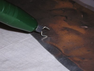
Figure 3. Measurement of Common Mode Signal due to ESD
Figure 4 shows the result of the
probe having just one tip touching the metal sheet,
as in Figure 3, while a contact discharge of an ESD simulator to its
own ground lead was made at 1 kV about a meter away from the probe. The
trace registers about +20 volts peak and slightly more than that in the
negative direction. A fast component of the signal at the start of the
ESD event shows about +14/-10 volt peaks. The actual start of the
ESD waveform is the first large positive peak of about +14 Volts. The
small noise before the first peak is direct EMI from the ESD simulator
radiating
directly into the scope vertical amplifiers. The ESD signal is delayed
by
the difference between the air path to the scope and the probe delay
including delay in cabling, about 16 nanoseconds in this case.
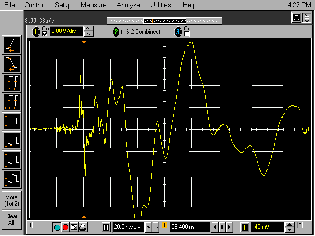
Figure 4. Probe Output With One Pin Touching Metal Plate - ~Common Mode Signal
(Vertical scale = 5 Volts/div, Horizontal scale = 20 ns/div)
(Vertical scale = 5 Volts/div, Horizontal scale = 20 ns/div)
Figure 5 shows the probe output with both pins touching the metal sheet,
as shown in Figure 1, under the same ESD conditions that generated Figure 4. The start of the ESD event is marked and
corresponds to the +14/-10 Volt peaks that started the ESD waveform in
Figure 4. There is clearly a significant amount of common mode rejection present. A
significant portion of the signal showing in Figure 5 is due to pickup
in the small loop formed by the probe tips. The probe common mode
rejection on its own would result in a somewhat smaller amplitude in
Figure 5. As it is, the remnant of the ESD signal is barely above the
EMI level shown by the scope itself. Keep in mind the contact discharge
was only about a meter from the scope and metal sheet.
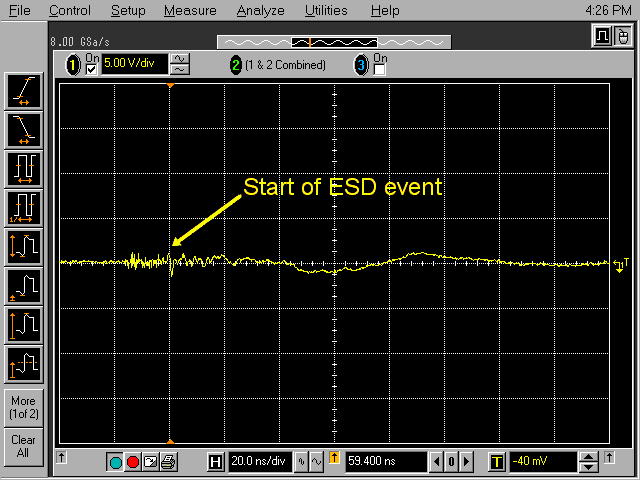
Figure 5. Probe Output With Two Pins Touching Metal Plate - Differential Signal
(Vertical scale = 5 Volts/div, Horizontal scale = 20 ns/div)
(Vertical scale = 5 Volts/div, Horizontal scale = 20 ns/div)
If the shield of the differential
probe cable is fastened 360 degrees to the equipment chassis (if
available) as the cable enters an equipment enclosure, the common mode
interference can be significantly reduced from the small levels of
Figure 5. I have made measurements with less than 100 millivolts
of measurement noise in the presence of a few kV of ESD using passive
differential techniques.
A lower frequency version of a passive differential probe useful to hundreds of MHz is described in my November 1994 article in the IEEE Circuits and Devices Magazine (~3.2 MB pdf file). A probe of this design as well as the higher frequency probe used in this article are available from Fischer Custom Communications.
A lower frequency version of a passive differential probe useful to hundreds of MHz is described in my November 1994 article in the IEEE Circuits and Devices Magazine (~3.2 MB pdf file). A probe of this design as well as the higher frequency probe used in this article are available from Fischer Custom Communications.
Summary:
Passive differential techniques can be used to make voltage
measurements in electronic equipment subjected to severe EMI where
active differential probes and single ended probes may not work. With careful design of a
measurement setup, measurement noise due to EMI can be reduced to the
point where logic signals may be measured in the face of severe EMI
such as ESD.
Other articles on this website related to this topic are:
- November 1994 article in the IEEE Circuits and Devices Magazine (~3.2 MB pdf file)
- July 1999: The Shorted Scope Probe Problem
- June 2000 supplement, Ground Lead, Friend or Foe?
- September 2001, Improving FET Probe Immunity to Unwanted Noise Pickup
- March 2003, Minimizing Errors in Oscilloscope Measurements
- November 2006, Measuring Signals in the Presence of Severe EMI - Part 1, How Not to Do It
- Data sheet for passive differential probe used in this article (~450 kB pdf file) by Fischer Custom Communications
- KeyTek MiniZap ESD Simulator
- Agilent 54845a Infiniium Oscilloscope
Click here for a description of my latest seminar to be available soon titled:
EMC
Lab Techniques for Designers
(How to find EMC problems and have some confidence your system will pass EMC testing while it is still in your lab).
(How to find EMC problems and have some confidence your system will pass EMC testing while it is still in your lab).
Home

