
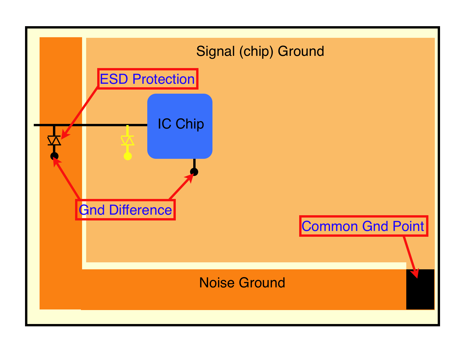
Figure 1. PCB Layout with Noise and Signal Ground Areas
Abstract: Printed Circuit
Board designers sometimes place protective devices on external signals
as they enter a PCB and shunt the current from these devices to a
separate "noise" ground distinct from the board signal ground. An
analysis is given that shows such a grounding structure can cause
problems in some cases and alternatives are suggested.
Discussion: Figure 1 shows
a PCB ground structure divided into two regions, signal ground
containing an IC chip, and "noise ground" containing a protective
device. Such a "noise" ground is often used for shunting currents
from protective devices where external signals enter the board. The two
grounds meet in the lower right hand corner of the board and from there
may connect to other system grounds.
In Figure 1, a signal is shown entering the board near the upper left hand side and immediately encountering a device used for ESD protection. The device shunts ESD or other impulsive currents into the noise ground to protect the IC chip and also keep the shunted current out of the thought to be sensitive signal ground. But there is a problem than can occur with this arrangement that may cause the protection to become ineffective and thus resulting in excessive voltage stress on the IC chip inputs.
As the shunted current flows from the protective device through noise ground to the common point, a voltage drop is generated across the noise ground path and is given by:
For fast currents, such as ESD, the Ri term can usually be dropped leaving just the Ldi/dt term. The inductance of the noise ground path is dependent on a number of factors, but if we assume a very conservative value of 20 nanohenries and also conservatively assuming an ESD event of about 2 kV generating a maximum di/dt of 6 Amps/nanosecond in the noise ground, we can calculate:
Since the IC chip is referenced through the signal ground back to the common point, the stress at the signal pin of the IC chip relative to its ground pin is the voltage across the protective device plus the Ldi/dt drop in the noise ground of 120 Volts. The Ldi/dt drop likely swamps out the drop across the protective device. In any event, the IC chip may be damaged in spite of the protective device because of the difference of ground potential between the protective device and the IC chip.
There are two possible fixes for this problem:
In Figure 1, a signal is shown entering the board near the upper left hand side and immediately encountering a device used for ESD protection. The device shunts ESD or other impulsive currents into the noise ground to protect the IC chip and also keep the shunted current out of the thought to be sensitive signal ground. But there is a problem than can occur with this arrangement that may cause the protection to become ineffective and thus resulting in excessive voltage stress on the IC chip inputs.
As the shunted current flows from the protective device through noise ground to the common point, a voltage drop is generated across the noise ground path and is given by:
e = L*di/dt + Ri
For fast currents, such as ESD, the Ri term can usually be dropped leaving just the Ldi/dt term. The inductance of the noise ground path is dependent on a number of factors, but if we assume a very conservative value of 20 nanohenries and also conservatively assuming an ESD event of about 2 kV generating a maximum di/dt of 6 Amps/nanosecond in the noise ground, we can calculate:
e = 20 nh * 6 Amps/ns = 120 Volts!
Since the IC chip is referenced through the signal ground back to the common point, the stress at the signal pin of the IC chip relative to its ground pin is the voltage across the protective device plus the Ldi/dt drop in the noise ground of 120 Volts. The Ldi/dt drop likely swamps out the drop across the protective device. In any event, the IC chip may be damaged in spite of the protective device because of the difference of ground potential between the protective device and the IC chip.
There are two possible fixes for this problem:
- Eliminate the separate ground areas on the board, forming one large ground area. This creates fewer problems than one might expect, in fact, often fewer than splitting the ground. But, in some systems there are legitimate reasons for a split ground structure, so if one cannot join the grounds then:
- Put a smaller secondary protective device (shown in yellow in Figure 1) close to the IC chip to protect it from the Ldi/dt generated voltage in the noise ground. The bulk of the current will be handled at the board edge by the main protective device, thus keeping most of the current out of the signal ground area. Some resistance could be added between the protective devices to insure most of the current is handled by the first protective device at the board edge.
Summary:
Sometimes splitting grounds can cause problems. In this case, splitting
noise and signal grounds reduced the effectiveness of ESD protection
for a board. Anytime PCB grounds are separated, a careful analysis
should be performed to make sure unexpected problems do not occur.
Additional articles on this website related to this topic are:
- August 2005, Off-spec Use of Protection Components
- February 2007, Coupled Bonding Conductors (from Lightning Protection to Noise Reduction)
- March 2007, Isolating Board and Chassis Grounds - A Potential Problem (An ESD Example)
Click here for a description of my latest seminar titled (now also available online as a WebEx seminar):
EMC
Lab Techniques for Designers
(How to find EMC problems and have some confidence your system will pass EMC testing while it is still in your lab).
(How to find EMC problems and have some confidence your system will pass EMC testing while it is still in your lab).
 |
Check
out my podcast containing mp3 format short tutorials, tech news and
more! Just click on the
microphone to see the listing
of free
audio programs. Content is added every week on technical
topics so check back frequently. |
Home